-
Mail Us Todaysales@efpcb.com
-
Company LocationShenzhen, Guangdong, China
-
+86-755-23724206Call us for more details
Part No.: E0415060189A
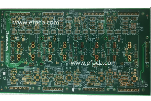
Layer count: 4 layer
Material: FR4, 1.6mm, 1 OZ for all layer
Minimum track: 5 mil
Minimum space: 5 mil
Minimum hole: 0.20mm
Surface finished: flash gold + Hard gold (Au>3um)
Panel size: 228*108mm/24up
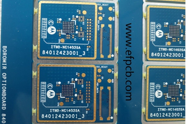
Selective hard gold PCBs are high-end variant of printed circuit boards that cater to high-end applications requiring exceptional durability and cost benefits. Since hard gold plating is only needed on the traces of PCB, not on the entire panel, it is more effective to plate hard gold on certain parts of PCB, which is so called selective hard gold plating. This is why selective hard gold PCBs are perfect for connectors, edge contacts, and other high-use areas in industries such as telecommunications, aerospace and semiconductor testing.
Developing a selective hard gold PCB is not an easy task. This article will go over the process of making a selective hard gold PCB, what factors to consider during design, and how to get the best results.
Selective hard gold PCB is the board where hard gold plating is applied to some areas including the edge connectors, contact pads, or high wear locations. Hard gold or electroplated gold is the typical surface finish of an aluminum electrolytic capacitor with a thick layer of gold alloyed with a small amount of nickel or cobalt to improve the hardness. Hard gold plating is very durable, resistant to wear, offers good salinity & corrosion protection, and has very good electrical conductivity. Though, gold is a costly commodity and plating the entire PCB surface with hard gold would add a significant amount to the cost of manufacturing. Hard gold plating can be economy applied to reduce cost and still obtain product performance for critical area.
Substrate Materials
The substrate material is the basis for a selective hard gold PCB. Manufacturers use FR4 for most general applications while high frequency laminates such as Rogers or PTFE for RF circuits or if using for semiconductor testing. The substrate must be able to serve as a plating base and the integrity of the substrate material should not be compromised in the subsequent processing and application.
Design Considerations
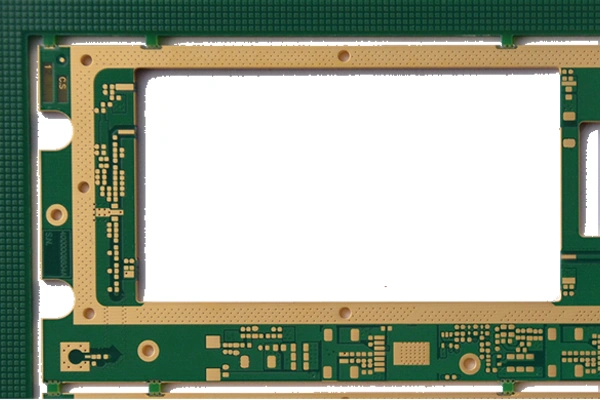
The selective hard gold PCB design must specify unique areas where hard gold plating is to be applied. Some of the most common ones include:
Manufacturers employ high-end CAD tools for PCB layout design and selective plating location definition. This allows hard gold finishing to be plated in only a certain position, and the remaining part of the PWB can have either HASL (Hot Air Solder Levelling) or ENIG (Electroless nickel immersion gold) more economical finishing.
Selective hard gold PCB manufacturing process
Pre-Production Preparation
Before the production starts, the design of the selective hard gold PCB will be carefully checked. The design is checked by the manufacturer to confirm that the areas that need to be plated with hard gold are properly identified. Photo tools are produced to control the plating and provide accurate application.
Copper Plating
The initial step of the physical manufacturing is copper plating. The conductive traces are formed by depositing a layer of copper onto the PCB substrate. This is usually done by electroplating, being that is when the PCB is dipped in a copper sulfate solution, and a current is passed.
Photoresist Application and Imaging
To get selective hard gold plating manufacturers use a photoresist on the surface of the PCB. This photosensitive agent is employed to cover the portions of the PCB that are not to be gold plated.
The photoresist is exposed to UV light through a photomask with the pattern that we want to produce. After exposure, the photoresist in the exposed areas is developed using a chemical solution and then copper traces and pads which are plated with hard gold are uncovered.
Nickel Plating
A layer of nickel is electroplated onto the exposed copper areas before the deposition of the hard gold layer. The nickel acts as a diffusion barrier to copper into the gold, and makes the plating more durable.
The nickel layer thickness is usually in the range of 100-200 μin (2.54-5.08 μm). Plating thickness and adhesion are tightly controlled by the manufacturer.
Finish hard gold plating
Then hard gold is electroplated onto the areas that were nickel-plated. The gold in this process contains a small amount of nickel or cobalt which makes it much harder and more wear resistant.
Depending on the application, the thickness of the hard gold layer generally ranges from 30 to 50 microinches (0.76 to 1.27 microns). For instance, semiconductor test boards are plated with thicker gold to enable them to make multiple mechanical contacts with the pins of IC packages and to provide long-term reliability.
Solder Mask Application
Once the hard gold plating process is done, a solder mask is placed on the PCB to protect the unplated portions of the board and to discourage solder bridging in the assembly process. The solder mask is normally printed by a screen printing method and then cured with UV or heat.
Surface Finish Inspection
The selective hard gold plating should be examined to confirm that it is up to the standards. Producers employ sophisticated instruments to measure, such as X-ray fluorescence (XRF) to test the thickness and consistency of the gold plating.
Testing and Quality Control
Electrical Testing
Selective hard gold PCBs can be tested electrically to verify the circuit. Continuity and impedance testing, amongst others, are carried out to test if the PCB meets the performance criteria.
Mechanical and Environmental Testing
Hard gold plating: the key to success of mechanical testing. Bend testing Wear testing, and, peeling strength testing are regularly used to test the mechanical properties of PCB. Environmental tests like thermal cycling and exposure to humidity make certain PCBs are able to hold up under severe conditions of use.
Selective hard gold PCBs have a number of benefits, such as:
Selective hard gold PCBs are used in many high reliability and high endurance applications. Including:
The selective hard gold PCB production process is challenging and requires high accuracy, professional knowledge, and hi-tech. From the choice and design of the materials used, to the process of electro-plating and the final testing, all steps need to be closely monitored if the wanted performance and durability is to be obtained. In such case it is very important to have a one of selective hard gold PCB manufacturer with experience in reliability critical applications like semiconductor testing boards. These manufacturers are equipped with specialized machinery and have expertise to produce high quality PCBs that can withstand even the toughest industry requirements.
Selective hard gold PCBs provide an economic alternative for applications that require strength and superior performance. Concentrating on critical plays allows the users to conserve materials, while producing reliable industrial products suitable for a variety of applications.