Comparison of Substrate Manufacturing Techniques and Their Applications
Keywords: IC Substrates China
With the continuous evolution of manufacturing techniques, the choice of substrate manufacturing method has a significant impact on the final product's quality, reliability, and performance. In this blog, we'll delve into a comparison of different IC Substrates China manufacturing techniques and explore their applications in various industries.
Substrate Manufacturing Techniques
- Printed Circuit Board (PCB) Manufacturing
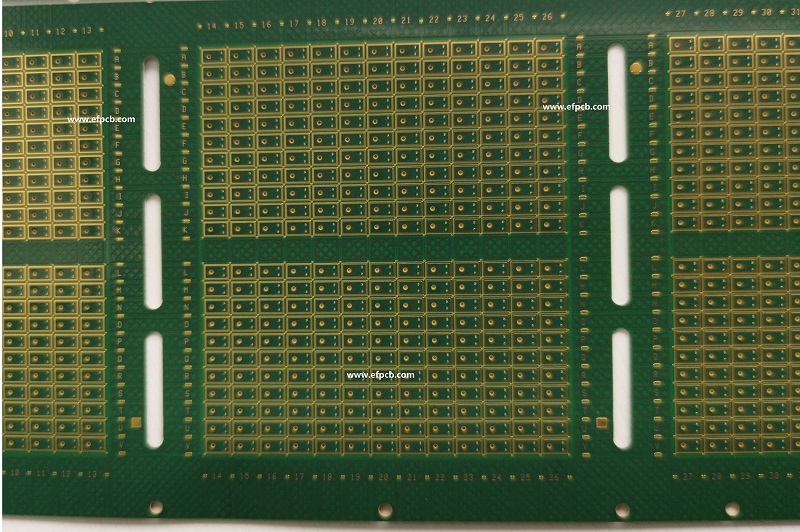
Printed Circuit Boards are perhaps the most widely recognized substrate manufacturing technique. PCBs are created by laminating layers of conductive copper tracks and insulating material (usually fiberglass) together. These boards are then etched to create circuit patterns. PCBs are commonly used in consumer electronics, computers, communication devices, and automotive electronics due to their cost-effectiveness, versatility, and ease of manufacturing.
- Ceramic Substrate Manufacturing
Ceramic IC Substrates China is very popular for extraordinary electrical insulation and thermal conductivity properties. These substrates are manufactured through processes such as tape casting, where ceramic materials are mixed, formed, and then sintered to achieve the desired properties. Ceramic substrates find applications in power electronics, LED modules, high-frequency communication devices, and aerospace components due to their ability to handle high temperatures and harsh environments.
- Flexible Substrate Fabrication
Flexible substrates, often made from polymer materials, are gaining traction due to their bendable and lightweight nature. Techniques like roll-to-roll (R2R) processing are used to manufacture these substrates at high speeds. Flexible substrates are used in wearable electronics, flexible displays, sensors, and medical devices where conformability and portability are essential.
- Semiconductor Wafer Substrates
Semiconductor substrates are typically silicon wafers on which integrated circuits are manufactured. The process involves growing a single crystal ingot and then slicing it into thin wafers. These wafers serve as the base for micro-fabrication processes like photolithography, etching, and deposition. Semiconductor substrates are essential for integrated circuits, microprocessors, memory devices, and sensors used in various electronic devices.
Applications of Different Substrate Manufacturing Techniques
- Consumer Electronics
PCBs are the go-to choice for most consumer electronic devices due to their cost-effectiveness and adaptability to high-volume production. They are found in smartphones, laptops, cameras, and gaming consoles.
- Communication Technology
High-frequency and microwave devices, such as radar systems and satellite communication equipment, rely on ceramic and semiconductor substrates for their superior electrical properties.
- Medical Devices
Flexible IC Substrates China are used in wearable health monitoring devices and medical sensors due to their comfort and ability to conform to the body's shape.
- 1Understanding UL 94V-0 Flammability Rating for Printed Circuit Boards (PCBs)
- 2HDI PCB Market Outlook 2025: Future Prospects, Growth Analysis & Innovations
- 3HDI PCB Design Comprehensive Guide: Mastering High Density Interconnect Technology in 2025
- 4Top 10 Flexible PCB Factories in 2025
- 5Top HDI PCB Manufacturers (2024)
- 6PCB core raw material CCL
- 7IC Substrate | Comprehensive Guide (2021)
- 8How to Make mSAP PCB?
- 9Top 10 IC Substrate Fabricators (2024)
- 10The Impact of Trump's Tariff Policy on Chinese PCB Industry and Countermeasures

- Skype ID: shawnwang2006
- Phone No。: +86-755-23724206
- Email: sales@efpcb.com
- Quick Contact