Concept of HDI PCB Manufacturing
Key Words: HDI PCB Manufacturing
What is importance of PCB ?
Printed circuit board is commonly known as PCB. Its role is very vital in the electrical and electronic industry. Conceptually, PCB is a board made up of a very thin flat metal or hard plastic type board and upon which so many electronic components are mounted. The prime function of the PCB is to provide mechanical support to the device. It has a major role in assisting electromagnetic shielding, heat transfer etc.
What is HDI PCB ?
With the pace and spirit of technological innovations, so many electronic products are being manufactured by the use of these advanced PCBs. HDI PCB is one of the technologically competent PCBs. For basic understanding, HDI stands for High Density Interconnector. In case of HDI PCB, it has a higher wiring density per unit area as opposed to conventional board. More specifically, HDI PCBs have finer spaces and lines, minor vias, capture pads and higher connection pad density. Generally, an HDI PCB has a symmetrical structure. In case of Unsymmetrical structure, the process is more cost effective.
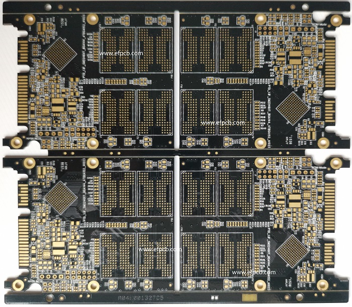
HDI PCB Manufacturing,
During HDI PCB Manufacturing, to achieve the HDI, it is taken care that the circuit board must have the extreme small PCB vias and fine traces. Each HDI PCB consists of inner and outer layers. The inner layers are the symmetry axis part of the PCB and more specifically, this part is penetrated by buried vias. The outer layers clamp the inner layers. The process of HDI PCB manufacturing differs based on the HDI builds. But the common manufacturing is sequential laminating. Besides sequential laminating, technologies for creating stacked vias and in-hole metallization are also very important in use.
In the end, it can be said that the process of manufacturing of HDI PCB is very important for getting the customized requirement. At the same time, a reliable HDI PCB manufacturer is equally important to be chosen.
- 1Understanding UL 94V-0 Flammability Rating for Printed Circuit Boards (PCBs)
- 2HDI PCB Market Outlook 2025: Future Prospects, Growth Analysis & Innovations
- 3HDI PCB Design Comprehensive Guide: Mastering High Density Interconnect Technology in 2025
- 4Top 10 Flexible PCB Factories in 2025
- 5Top HDI PCB Manufacturers (2024)
- 6IC Substrate | Comprehensive Guide (2021)
- 7PCB core raw material CCL
- 8How to Make mSAP PCB?
- 9Top 10 IC Substrate Fabricators (2024)
- 10The Impact of Trump's Tariff Policy on Chinese PCB Industry and Countermeasures

- Skype ID: shawnwang2006
- Phone No。: +86-755-23724206
- Email: sales@efpcb.com
- Quick Contact