Few Things You Might Have Missed Regarding HDI
Keywords: HDI PCB Manufacturing, High Volume PCB
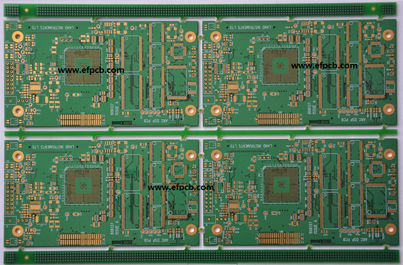
HDI, short for High Density Interconnection, is a type of printed circuit board technology that has started starting to develop at the end of 20th century. Mechanical drilling is utilized for traditional PCB boards, with few demerits that include high cost with aperture being 0.15mm and difficulty in improvement as a result of the influence of drilling tool. However, laser drilling is utilized for by HDI PCB Manufacturing and as soon as it was introduced, it received immense popularity. HDI boards are also referred as laser boards, which results in the fact that you can drastically decrease the pad size so that in each unit area more layout can be arranged. HDI technology pushes the development of PCB industry. Today in all kinds of devices HDI circuit boards have been massively applied.
In terms of board design and when compared with ordinary PCBs, the basic difference is that instead of through holes HDI PCBs obtain interconnections through blind holes and buried holes. In HDI PCBs design finer line width and smaller spacing are used so that you can fully use the space for layout and track. Therefore, High Volume PCB design novices should know how to distribute space for signal lines, how to switch applications of blind holes, buried holes and through holes, and how to arrange component space. Nevertheless, in the HDI PCB manufacturing process the first and uppermost job is to understand the corresponding process parameters.
In HDI PCB material few new requirements are brought which includes better size stability, antistatic mobility and non-adhesive. RCC is the typical material of HDI PCB. There're three types of RCC, namely Cast polyimide film, Polyimide metalized film, pure polyimide film.
The benefits of RCC include: light weight, excellent flexibility and flammability, small thickness, compatibility with characteristic impedance and excellent size stability.
In the process of HDI multi-layer PCBs, the role of traditional bonding sheet and copper foil is taken by insulating medium and conducting layer. Through traditional suppression technology RCC can be suppressed with the help of a chip. Then there is use of non-mechanical drilling method by HDI PCB Manufacturing such as laser so that micro-via interconnect can be formed.
- 1Understanding UL 94V-0 Flammability Rating for Printed Circuit Boards (PCBs)
- 2HDI PCB Market Outlook 2025: Future Prospects, Growth Analysis & Innovations
- 3HDI PCB Design Comprehensive Guide: Mastering High Density Interconnect Technology in 2025
- 4Top 10 Flexible PCB Factories in 2025
- 5Top HDI PCB Manufacturers (2024)
- 6PCB core raw material CCL
- 7IC Substrate | Comprehensive Guide (2021)
- 8How to Make mSAP PCB?
- 9Top 10 IC Substrate Fabricators (2024)
- 10The Impact of Trump's Tariff Policy on Chinese PCB Industry and Countermeasures

- Skype ID: shawnwang2006
- Phone No。: +86-755-23724206
- Email: sales@efpcb.com
- Quick Contact