Guidelines for High-Density Interconnect (HDI) PCB Design
Keywords: HDI PCB Manufacturing
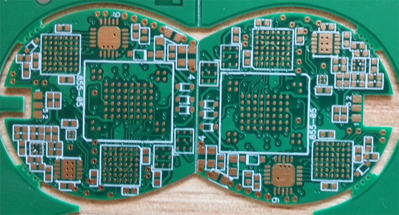
Before diving into the guidelines, it's essential to understand what High-Density Interconnect PCBs are. HDI PCBs are a specialized type of printed circuit board designed to provide increased component density and shorter signal paths. They achieve this by incorporating advanced design techniques and technologies, such as microvias, blind vias, and buried vias. These boards are especially suited for high-frequency and high-speed applications, making them a favorite in industries like aerospace, medical devices, and telecommunications. Here is the design aspect of HDI PCB Manufacturing.
HDI PCB Design Guidelines
Layer Stackup Planning: Selecting the right materials and layer configurations can significantly impact signal integrity and thermal management.
Microvias and Staggered Vias: Microvias are tiny holes used to connect different layers in an HDI PCB. Staggered vias, which overlap rather than align, can reduce the chances of signal interference. Utilizing microvias and staggered vias allows for a high-density interconnection of components, but it requires careful planning to prevent potential manufacturing and reliability issues.
Signal Integrity: HDI PCBs often find applications in high-frequency systems where signal integrity is paramount. Proper impedance control, the careful placement of components, and routing traces are essential for maintaining signal quality. Use high-quality materials that provide consistent dielectric properties.
Thermal Management: Effective thermal management in HDI PCB Manufacturing is critical to ensure the long-term reliability of the board. Incorporate heat sinks, thermal vias, and consider the location of components that generate the most heat.
Design for Manufacturing (DFM): DFM principles are crucial when designing HDI PCBs. Consult with your manufacturer early in the design process to ensure that your design can be manufactured efficiently and reliably. Addressing manufacturing concerns at the design stage can save time and costs in the long run.
Component Placement: Careful component placement is essential in HDI PCBs. Optimize the arrangement to minimize signal paths, reduce crosstalk, and ensure efficient routing. Use specialized design software that helps with auto-placement to maintain accuracy and efficiency.
Routing and Trace Widths: Ensure that your routing adheres to design rules, and use appropriate trace widths and spacing to maintain signal integrity and reduce signal loss. Differential pair routing is crucial for high-speed designs.
Testing and Verification: Implement comprehensive design rule checks (DRC) and use simulation tools to evaluate signal integrity, thermal performance, and manufacturability in HDI PCB Manufacturing. Prototyping and testing can help identify and address issues early in the design process.
- 1Understanding UL 94V-0 Flammability Rating for Printed Circuit Boards (PCBs)
- 2HDI PCB Market Outlook 2025: Future Prospects, Growth Analysis & Innovations
- 3HDI PCB Design Comprehensive Guide: Mastering High Density Interconnect Technology in 2025
- 4Top 10 Flexible PCB Factories in 2025
- 5Top HDI PCB Manufacturers (2024)
- 6IC Substrate | Comprehensive Guide (2021)
- 7PCB core raw material CCL
- 8Top 10 IC Substrate Fabricators (2024)
- 9How to Make mSAP PCB?
- 10The Impact of Trump's Tariff Policy on Chinese PCB Industry and Countermeasures

- Skype ID: shawnwang2006
- Phone No。: +86-755-23724206
- Email: sales@efpcb.com
- Quick Contact