Have some familiarity with the Backplane PCB Fabrication and Testing
Keywords: Backplane Board, Backplane PCB
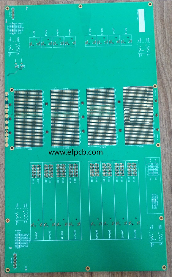
Containing attachments and openings to interconnect different gadgets or PCB gatherings in lined up with one another a backplane is an electronic framework. For an electronic framework, Backplane PCB behaves like a Backbone and to each space; it disperses low-voltage power.
The working of inactive electronic parts like diodes, capacitors, and resistors as well as backplanes is assessed by Backplane testing. The electrical and actual associations between framework parts are given by the backplane. Fundamental inside its recommended boundaries, it is working. A few tests are performed to guarantee the smooth working of a backplane. Backplane testing is known as the most common way of distinguishing the significant deficiencies in the backplane by utilizing test processes.
Most extreme voltage, test opposition, test focuses and greatest current are remembered for Key Specifications of backplane testing.
Following kinds of tests are available in Backplane PCB Testing:
Visual Inspection: For right position, parts on the backplane are really taken a look at exclusively in this test. Checking part direction and patch joints are incorporated. It very well may be finished through Automated Optical Inspection (AOI) or physically.
Electrical Tests: By sending an electrical flow through the follows and nails to the board, these test actually takes a look at the associations. Two significant regions to test are:
• To guarantee that there is no association, Short or Isolation which implies there is a space between the pins.
• Open circuit or Continuity which implies there is an association between the pins.
In two terms, the electrical test gives affirmation. On the off chance that an association exists between the test focuses, it is Continuity and if doesn't, it is Short. Since an association which isn't needed can make obstruction on the board and lead glitches, this test is fundamental.
Signal Integrity Analysis and Simulation: As inside the backplanes, higher speed signals are comprised. For the recurrence space and time area estimations, network analyzers are utilized to examine such signals.
Useful Test: For checking how the hardware will function in the wake of coordinating with the application or planned last gadget, this test is finished.
Key Tips and Difficulties for Backplane PCB Fabrication
For conveying capability loads up including line cards or little girl loads up Backplane PCB, likewise known motherboard, is a sort of baseboard dependable. Conveying girl loads up and circulating ability to workloads up is the significant undertaking of backplane load up so that signal transmission and electrical association can be accomplished. Subsequently through the participation between its daughterboard and backplane, the framework capability can be gained.
The backplane load up capabilities continuously cover power appropriation, signal transmission and capability load up conveying as IC part includes progressively higher respectability. Along with fast headway that is made in electronic get together, the advancement of rapid digitalization and high recurrence of sign transmission, the I/O count continues to rise. Backplane loads up need to arrive at higher necessity to execute those capabilities as far as sign transmission quality, load up thickness, layer count, dependability, by means of count and recurrence.
Appropriately, Backplane PCB creation must be defied with thorough test on stub, load up size, load up thickness, arrangement control, layer count and back penetrating profundity to acquire such high prerequisite in execution. At the end of the day, taking everything into account, every one of the referenced perspectives are most certainly main points of contention. To show the key hardships met in backplane PCB manufacture process, this article points and in light of PCB, here you can talk about a few convenient tips.
1. Penetrating Technology
Penetrating is conceivably excessively short to arrive at the load up because of high thickness of backplane load up. Anyway during boring cycle, too lengthy penetrating instrument will in general experience the ill effects of breaking. Emphatically limiting backplane PCB execution, a lot of residue might impede the burr and opening might be caused moreover.
Tips
• Through the utilization of profundity control in a conductive manner, Drilling profundity can still up in the air.
• In view of the opening bored through X-beam penetrating, CCD strategy ought to be applied in boring CCD marker and backplane load up.
2. Arrangement Control
Taking everything into account, Alignment control is the preeminent assembling trouble as terrible arrangement control will perhaps prompt shorts.
Various methodology and components influences arrangement control among which layer stack-up most matters. Three kinds of structures are available normally in Multi-layer PCBs: thermocouple warming, pin-lam and mass-lam.
Tips
• Pins classification decision utilized is very vital as pin-lam stack-up is utilized. For instance, we view that as viable with the necessity on arrangement control, four pins are utilized to perform better compared to eight round pins.
• Copper-iron bolts in addition to short dowels will be a decent choice when pin-lam can't be applied because of certain impediments.
• In pin-lam, the ideal piece strategy lies as it will not excite shock impact on center board.
3. ICD Analysis
During the course of high-recurrence material manufacture, ICD will in general be happened causing emotional quality gamble on long haul dependability and electrical association. So that such issues can be kept away from in the backplane PCB fabricating process, the ICD cause and its answer should be summed up. Lacking wiping is completed and sap gel buildup left on internal copper layer is the causes behind ICD issue.
Tips
• To confirm that gel buildup has been wiped out, boring boundary control ought to be enhanced.
• To stop tar because of deficient maturing being left on inward copper layers, Board material maturing degree ought to be investigated.
4. Electroplating Capability
The angle proportion will be high also Due to high thickness of backplane load up. For guaranteeing adequate copper at opening, adequate copper will be inside opening in the event that the electroplating isn't sufficiently profound. Opening is impacted, contrary copper thickness at opening wall and driving by means of gap is come about if an excessive amount of copper will be left at opening mouth.
Tips
• New DC plating arrangement should be utilized.
• With DC plating arrangement, Pulse plating arrangement ought to be analyzed regarding arrangement solidness, unwavering quality and plating ability.
5. Back penetrating Stub
Stub will prompt even sign transmission disappointment or motion toward be mutilated, taking everything into account. In this manner, stub on fast sign transmission ought to be explained the adverse consequence brought about by. At the point when the length of stub is under 0.25mm, its impact on signal is can be overlooked and very low up to now. Inside 0.25mm, stub length ought to be controlled subsequently in Backplane PCB.
- 1Understanding UL 94V-0 Flammability Rating for Printed Circuit Boards (PCBs)
- 2HDI PCB Market Outlook 2025: Future Prospects, Growth Analysis & Innovations
- 3HDI PCB Design Comprehensive Guide: Mastering High Density Interconnect Technology in 2025
- 4Top 10 Flexible PCB Factories in 2025
- 5Top HDI PCB Manufacturers (2024)
- 6IC Substrate | Comprehensive Guide (2021)
- 7PCB core raw material CCL
- 8How to Make mSAP PCB?
- 9Top 10 IC Substrate Fabricators (2024)
- 10What is IPC 4761 Type VII Via in Pad PCB?

- Skype ID: shawnwang2006
- Phone No。: +86-755-23724206
- Email: sales@efpcb.com
- Quick Contact