How to Develop a Working PCB
 Printed Circuit Boards (PCBs) are rugged nonconductive boards built on substrate-based structures. To the electrical components of a circuit, the flexible PCB is mainly used to provide electrical connection and mechanical support. In electronic devices, they are quite prevalent and in most cases, they are easily identified as the green-coloured board. Generally, a PCB consists of tons of active and passive components. On the circuit board, these parts are connected with traces. Several procedures are involved with the production of printed circuit boards
The form factor is defined as a feature of any hardware design that specifies the shape, size, and other relevant physical properties of the Rigid Flex PCB in its entirety. Aspects such as mounting schemes, board configurations and chassis, are taken into consideration while determining a form factor of a PCB design. With copper interconnects (routes) the connection among the components on a PCB is established, which then act as the pathway for the electrical signals.
Developing Steps of PCB
At first, a design specification (document) is written that recognizes the required functionality of the PCB. Through this, the designer creates the circuit design, which is then entered into the PCB design tools.
• Through simulation using a suitably defined test stimulus the design schematic is analyzed, and the operation of the design is then verified. According to the required specification if the design is not meet, then either the design must be modified, or in maximum cases, the design specification must be changed.
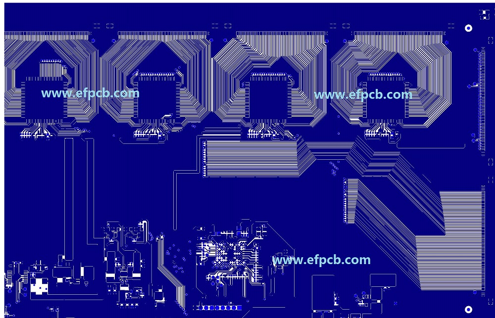
•The PCB layout is created when the design schematic is completed and then layout directives (set by the particular design project) and the manufacturing process design rules are taken into account.
•After successful completion of the Flex Circuits Board layout, it undergoes analysis by (i) simulating the schematic design to account for the track parasitic components (usually the parasitic capacitance is used), and (ii) confirming whether the circuit design of PCB will function correctly by using specially designed signal integrity tools. If not, then the design layout, schematic, or specification will need modification.
The design is ready for submission for manufacturing after all steps to the layout have been completed.
- 1Understanding UL 94V-0 Flammability Rating for Printed Circuit Boards (PCBs)
- 2HDI PCB Market Outlook 2025: Future Prospects, Growth Analysis & Innovations
- 3HDI PCB Design Comprehensive Guide: Mastering High Density Interconnect Technology in 2025
- 4Top 10 Flexible PCB Factories in 2025
- 5Top HDI PCB Manufacturers (2024)
- 6PCB core raw material CCL
- 7IC Substrate | Comprehensive Guide (2021)
- 8How to Make mSAP PCB?
- 9Top 10 IC Substrate Fabricators (2024)
- 10The Impact of Trump's Tariff Policy on Chinese PCB Industry and Countermeasures

- Skype ID: shawnwang2006
- Phone No。: +86-755-23724206
- Email: sales@efpcb.com
- Quick Contact