How to Generate Circuit Pattern and Learn the Preparation of the Base Material
Keywords: Rigid Flexible PCB Manufacturer, Rigid Flex PCB
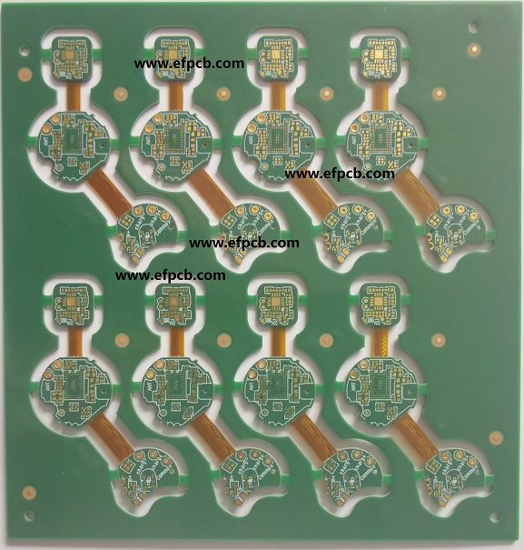
There are so many PCB manufacturers who never realize that a rigid flex PCB is complex and it needs a hell lot of communication between them and the consumers. Between the designer and the rigid-flex PCB manufacturer, there had to be a few early discussions.
This article will tell you about the steps involved in rigid-flex PCB manufacturing that you need to carry out with precision.
Cleaning and Preparing the Base Material of Rigid-flex PCB
By cleaning/preparing laminates for rigid-flex boards, you can begin the manufacturing of rigid-flex boards. Laminates have copper layers and they have an adhesive coating on them. You need to carefully scrub it before you use it in the further rigid-flex PCB manufacturing process.
This type of pre-cleaning is so very important because generally, the covering of copper coil is done with an anti-rust layer for oxidation protection. But this protective layer results in being an obstacle to rigid flexible PCB manufacturer, and yes you have to deal with it.
PCB manufacturers follow three steps that are -
At First, you have to completely immerse the copper foil in an acid solution, and in case you are unable to do it then spray the acid.
Next, companies treat the copper coil with the solution of sodium persulfate so that you can micro etch it.
At last, with the help of an appropriate kind of oxidant you have to coat the coil extensively. This prevents oxidation and adhesion to a great extent.
How To Generate Circuit Pattern for the Rigid-flex PCB
Generating circuit patterns is the second step in manufacturing a Rigid Flex PCB board. With the help of two given methods, you can generate circuit patterns:
Screen printing-This method helps you in producing the much-desired circuit deposits/patterns on the surface of the laminate.
Photographic imaging- This technology is used since the ancient period, but still, it is very famous for drawing circuit patterns on the surface of laminates. You have to place the dry photoresist film that consists of the desired circuit pattern. After this, you have to expose this component to ultraviolet light.
This will make sure that the circuit pattern gets transferred from the photomask to the laminate. At last, for removing the film you will require the use of chemicals in rigid flex PCB.
- 1Understanding UL 94V-0 Flammability Rating for Printed Circuit Boards (PCBs)
- 2HDI PCB Market Outlook 2025: Future Prospects, Growth Analysis & Innovations
- 3HDI PCB Design Comprehensive Guide: Mastering High Density Interconnect Technology in 2025
- 4Top 10 Flexible PCB Factories in 2025
- 5Top HDI PCB Manufacturers (2024)
- 6IC Substrate | Comprehensive Guide (2021)
- 7PCB core raw material CCL
- 8How to Make mSAP PCB?
- 9Top 10 IC Substrate Fabricators (2024)
- 10What is IPC 4761 Type VII Via in Pad PCB?

- Skype ID: shawnwang2006
- Phone No。: +86-755-23724206
- Email: sales@efpcb.com
- Quick Contact