How to Make mSAP PCB?
The Modified Semi-Additive Process (mSAP) developed has revolutionized the PCB manufacturing industry with the production capacity of ultra-thin and high density interconnects (HDI) required by the electronic industry. With the small, powerful yet sophisticated devices becoming the order of the day, the mSAP PCBs are the mainstay for the cutting-edge technologies such as smartphones, wearable gadgets, IoT applications as well as automotive electronics. This report offers a comprehensive review of mSAP PCB manufacturing in 2025, detailing the main processes, materials, challenges, and trends in the industry.
What is mSAP PCB?
mSAP PCB Mean modified semi-additive process printed PCB, a most advanced technology, that allows for even finer circuit lines and spaces that standard subtractive method boards. Instead of subtractive methods that etch copper away to create circuits, mSAP deposits copper to build the circuit patterns in a more controlled way, with greater precision and material efficiencies.
This is especially critical for applications with a high wiring density, such as 5G handsets, high throughput processors, and small consumer products. It is now 2025 and miniaturization and performance are still driving the requirement for mSAP boards.
Key Advantages of mSAP PCB
There are many advantages that have prompted the industry to adopt mSAP PCB manufacturing instead of the normal approach:
- Higher Density: Ultra-fine lines circuit (<10μm) can be coated out by mSAP, which is best suited for HDI applications.
- Better Signal Integrity: Accurate control of a circuit pattern reduces signal loss and interference, which is essential in high-frequency applications such as 5G.
- Cost Control: mSAP requires less copper than subtractive techniques, to reduce waste and cost.
- Small Form Factor: Being able to make thinner and light boards is becoming ever more important with the arrival of miniaturized electronic devices.
- Environmental advantages: By using less chemicals and generating fewer wastes mSAP is also better for the environment.
Materials for mSAP PCB Production
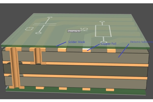
The choice of materials in mSAP PCB fabrication is supposed to contribute significantly to product performance and reliability. Key materials include:
- Copper foil: Conductive layers are usually formed with ultra-thin copper foils having a thickness of, for example, 9~μ m or below.
- Dielectric Substrates: Polyimide, Liquid Crystal Polymer (LCP), modified epoxies, are high-performance dielectric materials that serve as both the insulating layer and structural support. Chemically Deposited Copper: A conductive layer (plate) that is initiated into a surface of equal potential.
- Solder Mask: A material that is sensitive to light and is used to pattern the circuits in photolithography.
- Surface Finishes: Protective layers such as ENIG (Electroless Nickel Immersion Gold) or OSP (Organic Solderability Preservative) cover are applied to achieve solderability and to keep the board from oxidizing.
Process of mSAP PCB Manufacture
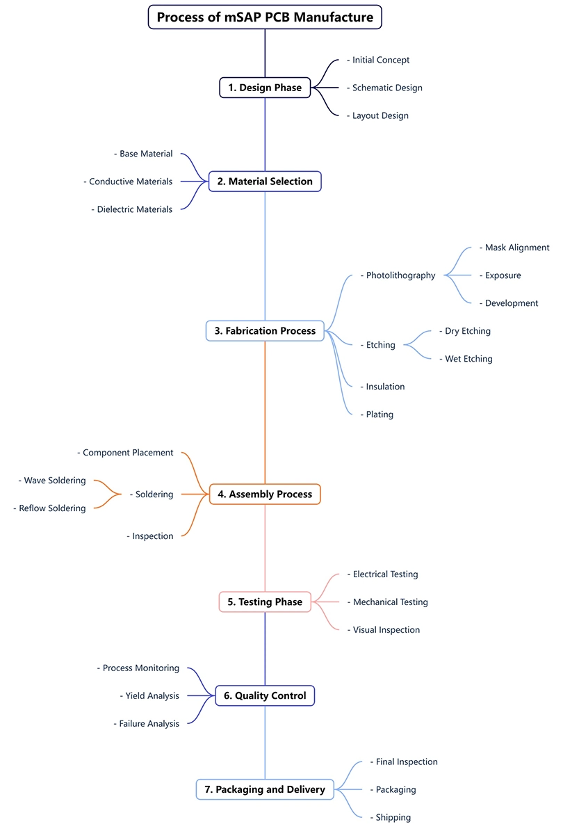
Manufacturing of the mSAP PCB is an intricate, reliable and controlled process. Here is a full breakdown of every step:
1. Substrate Preparation
The process starts with preparation of the base substrate made of dielectric material with very thin copper foil covering. The substrate is cleansed and treated for appropriate bonding of the following layers.
2. Electroless Copper Plating
An electroless copper thin layer is coated on the substrate. This step forms a continuous conductive material layer as a base for the circuit patterns.
3. Photoresist Application
A patterned photoresist film is deposited on the substrate. The photoresist is thereafter exposed to ultraviolet (UV) light through a photo mask which defines the circuit pattern to be etched. Exposed parts become solid, and not exposed parts stay essentially soluble.
4. Development and Etching
The unexposed photoresist is stripped away, exposing the underlying copper. This is followed by etching in which the copper exposed by the resist is chemically dissolved to form the circuit pattern (superposed and protected by the hardened photo-resist.
5. Semi-Additive Plating
In this crucial step, more copper is electrodeposited on the bare circuit lines to build up a thickness and conductivity. The semi-additive process enables superior dimensions control of the circuit pattern.
6. Photoresist Stripping
The hardened photoresist is then removed, revealing the original thin copper layer underneath. This layer is subsequently etched off leaving only thicker, plated copper traces.
7. Surface Finishing
A protective finish is treated for oxidation and solderability. The popular surface finishes on boards of mSAP for 2025 are ENIG, immersion silver, and OSP.
8. Quality Inspection
The last stage is strictly quality control to be sure the mSAP PCB fit design rules and standards. Defect and performance testing are typically implemented and achieved through techniques such as automated optical inspection (AOI), X-ray imaging, and electrical testing.
mSAP PCB Manufacturing Difficulties
Nevertheless, mSAP PCB fabrication is not free of challenges. These include:
- Cost: The technological tools and resources needed for mSAP techniques can incur a high initial investment.
- Process Complexity: Perecision control and expertize is requred to hold lines and spaces on single digit micron levels of production.
- Material Compatibility: It may be difficult to adhere layers together correctly, and they may be incompatible with high-frequency signals.
- Environmental Regulations: Political and environmental changes will continue to exert pressure on the processing of heavy metals as govemment regulations become more stringent.
Industry Trends and Innovation 2025
The mSAP PCB market is on a growth mode so as to keep up with the evolving requirements of advance technologies. Major trends and innovation in 2025 are:
- 5G and 5G+: These Devices need high-frequency capabilities and low signal loss mSAP PCBs.
- Advanced Packaging: There are now more integrations with advanced packaging technologies, like system-in-package (SiP) and chiplets.
- Sustainability: Makers are finding more sustainable ways to produce copper, by recycling, and less environmentally destructive ways to mine and process it, cutting waste flows and chemical inputs.
- Automation and AI: The adoption of artificial intelligence and automation on production lines is increasing efficiency and decreasing defects.
- Ultra-Flat Features: With slimmer, sleeker device models in demand, substrate materials and manufacturing methods are being refined. Applications of mSAP PCB
mSAP PCBs are flexible and are appropriates to various end-uses such as:
- Smart Phones: Compact design and functionality demand high density interconnects.
- Wearables: Fitness trackers and smartwatches can benefit from ultra-thin and flexible mSAP PCBs.
- Automotive Electronics: ADAS and infotainment systems employ mSAP PCBs.
- IoT Devices: Small and efficient form factors enable the expanding IoT market.
- Medical Devices: Diagnostic equipment, implants and other devices benefit from the precision and reliability of mSAP PCBs.
Conclusion
mSAP PCB fabrication is increasingly avery core ofy, enabling production of high performing, miniaturized and high reliable devices. Through the use of advanced materials, processes and technologies, they’ll be ready to rise to the challenges of 2025 and beyond.
The significance of mSAP PCB technology will only increase as industries are further pushing the envelope in miniaturization and performance. From faster 5G connectivity to the next generation of IoT devices, mSAP PCB fabrication is leading the charge.
With deeper knowledge of the mSAP process and industry trends, companies can be well equipped to succeed in mSAP, a fiercely competitive industry landscape that is evolving at lightning speed.
- 1Understanding UL 94V-0 Flammability Rating for Printed Circuit Boards (PCBs)
- 2HDI PCB Market Outlook 2025: Future Prospects, Growth Analysis & Innovations
- 3HDI PCB Design Comprehensive Guide: Mastering High Density Interconnect Technology in 2025
- 4Top 10 Flexible PCB Factories in 2025
- 5Top HDI PCB Manufacturers (2024)
- 6PCB core raw material CCL
- 7IC Substrate | Comprehensive Guide (2021)
- 8How to Make mSAP PCB?
- 9Top 10 IC Substrate Fabricators (2024)
- 10The Impact of Trump's Tariff Policy on Chinese PCB Industry and Countermeasures

- Skype ID: shawnwang2006
- Phone No。: +86-755-23724206
- Email: sales@efpcb.com
- Quick Contact