Learn About HDI Printed Circuit Board
Keywords: HDI PCB Manufacturing
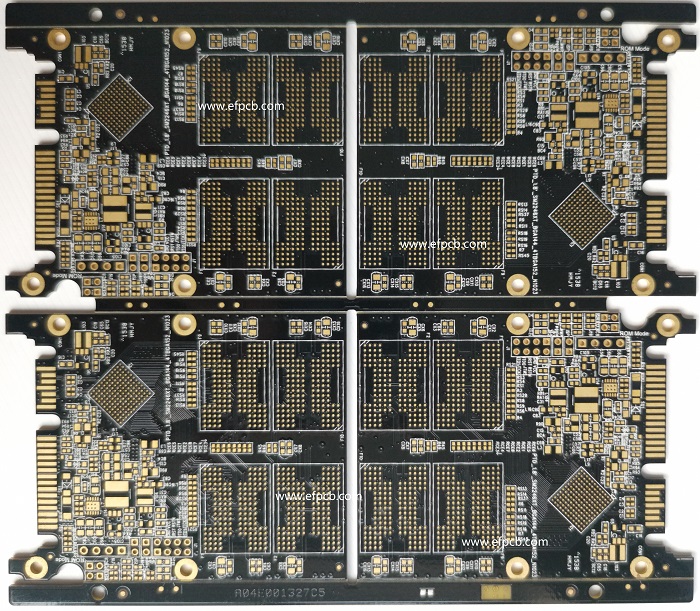
Contrasted with standard printed circuit sheets, HDI Printed Circuit Sheets are those which use a bigger number of interconnections. In HDI PCB Manufacturing, gadgets fashioners and engineers utilize a HDI printed circuit board to be unified with a pin thickness. The significant traits of HDI printed circuit sheets are that they incorporate denser circuit interconnections and thick part position. It then, at that point, considers decreases in the bundle size or impression of the electronic congregations that is produced using HDI printed circuit sheets. In the event of elite execution gadgets this innovation has empowered size decreases in purchaser items, for example, cell phones, contact screens like utilized in tablet PCs, PCs computerized cameras.
A portion of the nuts and bolts of HDI PCBs that incorporates their turn of events, measurements, phrasing and benefits is evaluated by this article.
Advancement of HDI Printed Circuit Board
HDI PCB Assembling organization created HDI printed circuit sheets. It was done in light of the fact that there was need to give an expanded degree of computational power and execution. By enterprises, for example, broadcast communications this need was driven generally, where the push to give more modest and all the more impressive cell phones required figuring out how to bundle more electronic hardware in a more modest, denser bundle. Not many of these key IC innovation patterns comprises of:
• There are quicker signal ascent times
• The contracting size of doors
• In controlling power dissemination there is decrease in working voltage levels
• More elevated levels of door joining
• Decrease in kick the bucket size
There is moving of the pattern and bundling of ICs in HDI PCB Assembling. It is finished from the utilization of low-count fringe lead outline bundles towards surface mount innovation. Under the whole surface region of the IC, it then permits the position of interconnecting pins. Ball Matrix Exhibit (BGA) is one such innovation, which in a framework design on the underside of the IC places the interconnecting pins. The relating thickness of pins increments as an ever increasing number of pins are added to the IC bundles, and there is decline in the layered dividing for the circuit board follows or cushions here.
- 1Understanding UL 94V-0 Flammability Rating for Printed Circuit Boards (PCBs)
- 2HDI PCB Market Outlook 2025: Future Prospects, Growth Analysis & Innovations
- 3HDI PCB Design Comprehensive Guide: Mastering High Density Interconnect Technology in 2025
- 4Top 10 Flexible PCB Factories in 2025
- 5Top HDI PCB Manufacturers (2024)
- 6IC Substrate | Comprehensive Guide (2021)
- 7PCB core raw material CCL
- 8Top 10 IC Substrate Fabricators (2024)
- 9How to Make mSAP PCB?
- 10The Impact of Trump's Tariff Policy on Chinese PCB Industry and Countermeasures

- Skype ID: shawnwang2006
- Phone No。: +86-755-23724206
- Email: sales@efpcb.com
- Quick Contact