Mastering RF PCB Troubleshooting and Debugging

Keywords: RF PCB
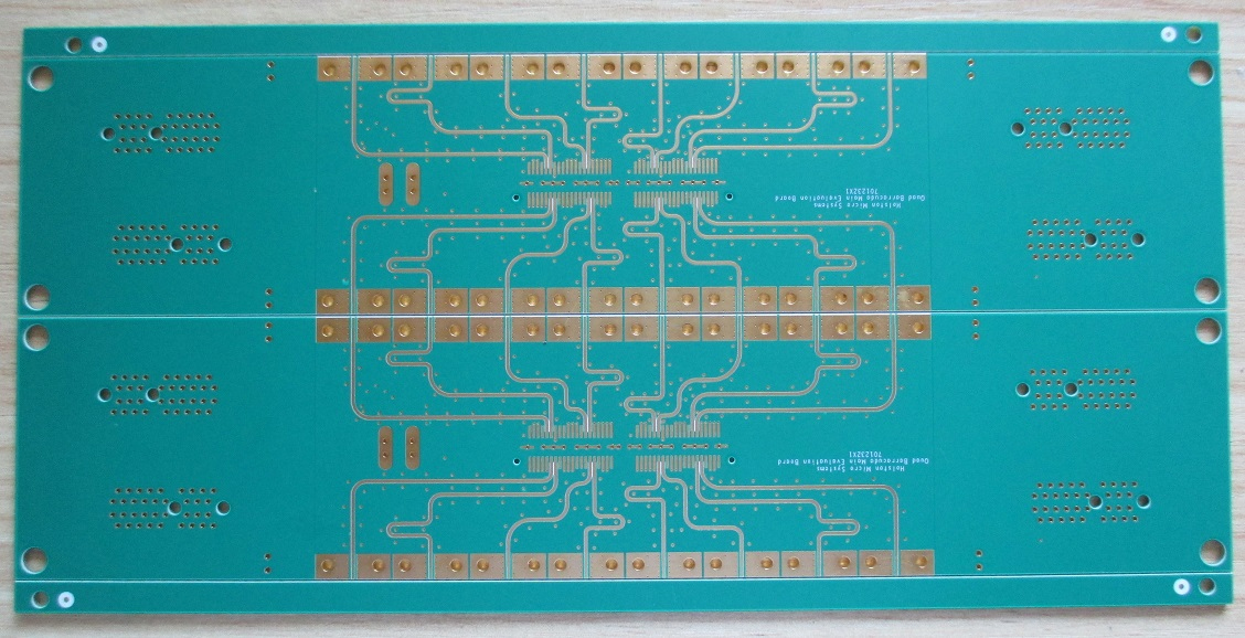
Radio frequency PCBs handle signals in the RF spectrum, typically ranging from a few megahertz (MHz) to several gigahertz (GHz). These boards are found in various applications, from wireless communication devices to radar systems and more. Due to the high-frequency nature of RF signals, their behavior can be influenced by a myriad of factors, making RF PCB particularly susceptible to problems. Let's delve into the art of RF PCB troubleshooting and debugging.
Common RF PCB Issues
Signal Integrity Problems: RF signals are highly sensitive to impedance mismatches, reflections, and signal loss. These issues can result in poor performance, dropped calls, or data loss in RF communication systems.
Noise and Interference: RF circuits are prone to external noise and interference from nearby components or external sources. These disturbances can disrupt the intended signal path and degrade performance.
Connector and Cable Issues: Connectors and cables are critical components in RF systems. Poorly connected cables or damaged connectors can lead to signal loss and intermittent performance.
Component Problems: Faulty RF PCB components, such as amplifiers, mixers, or filters, can significantly impact the overall system performance.
Power Supply Issues: Stable power supply is crucial for RF circuits. Voltage fluctuations or noise in the power source can lead to RF signal distortion.
RF PCB Troubleshooting and Debugging Techniques
Spectrum Analyzer: Use a spectrum analyzer to visualize the RF signals on the board. This tool is able to help identify unwanted harmonics, noise, and interference.
Network Analyzer: A network analyzer is valuable for measuring impedance mismatches and analyzing the S-parameters of RF components and traces.
Oscilloscope: While traditional oscilloscopes have limited bandwidth, high-frequency oscilloscopes are available for probing RF signals. They can help you assess signal quality and identify anomalies.
Near-Field Probing: This technique involves using a near-field probe to detect electromagnetic fields and pinpoint sources of interference or unintended radiation.
Smith Chart Analysis: Smith charts are excellent tools for impedance matching. Utilize them to determine the optimal impedance for RF components and connections.
Antenna Pattern Measurement: In wireless communication devices, antenna pattern measurement can identify issues with radiation patterns and coverage.
Simulation and Modeling: RF simulation software can help you assess the performance of your RF PCB design virtually. It allows you to predict potential issues before fabrication.
- 1Understanding UL 94V-0 Flammability Rating for Printed Circuit Boards (PCBs)
- 2HDI PCB Market Outlook 2025: Future Prospects, Growth Analysis & Innovations
- 3HDI PCB Design Comprehensive Guide: Mastering High Density Interconnect Technology in 2025
- 4Top 10 Flexible PCB Factories in 2025
- 5Top HDI PCB Manufacturers (2024)
- 6PCB core raw material CCL
- 7IC Substrate | Comprehensive Guide (2021)
- 8How to Make mSAP PCB?
- 9Top 10 IC Substrate Fabricators (2024)
- 10The Impact of Trump's Tariff Policy on Chinese PCB Industry and Countermeasures

- Skype ID: shawnwang2006
- Phone No。: +86-755-23724206
- Email: sales@efpcb.com
- Quick Contact
