PCB Assembly Processes Types and Reason for Expensive PCBA
Keywords: PCB Assembly, PCB Assembly China
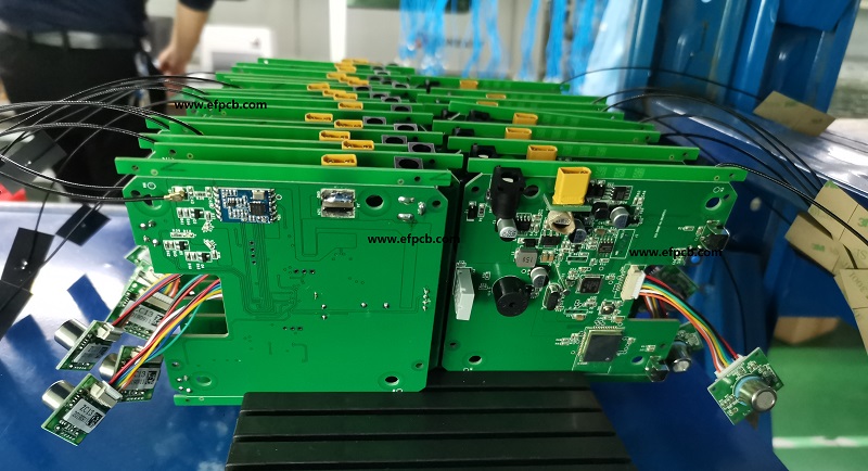
The term PCB Assembly process or PCBA refers to the manufacturing procedure for an assembled PCB. The necessary electronics components are installed on the PCB during this operation. Traces, or copper wires on a bare board, are used to electrically connect connections and components.
Various traces transmit signals between these components, enabling the circuit board to operate in a way that was particularly intended. There are both automated and manual stages involved in PCB construction. A board maker has both manual and automated choices for every stage of the process.
We will talk about the three fundamental technologies used in the PCB assembly process in this post.
- Process for Thru-Hole Technology (THT) Assembly
- Process of assembly for Surface Mount Technology (SMT)
- Technology Mix
Using Through-Hole Technology (THT) for PCB Assembly
Pin-through-hole (PTH) components are placed into electronic circuits using the Through Hole Technology (THT) technique, which involves drilling holes into printed circuit boards (PCBs).
The ends, or leads, are then connected to pads on the opposing side using wave soldering or reflow soldering tools and molten metal solder. It is additionally known as through-hole assembly, this method.
Following are the three essential processes in the assembly process for Through Hole Technology (THT):
Placement of Components.
- Step 1
Engineers working in the field manually do this procedure. Engineers must rapidly and accurately insert components on the PCB according to the client's PCB design files. To ensure high-quality finished goods, component placement must adhere to the rules and operating criteria of the through-hole mounting procedure.
- Step 2: Inspection and correction
Once the component placement is complete, the board is put in a transport frame that matches it, where it will be automatically checked to see if the components are correctly plugged in. If component placement problems are discovered, it is also simple to have them quickly fixed. After all, in the PCBA process, this occurs before soldering.
- Step 3: wave soldering
Now, carefully solder the THT components to the circuit board. In the wave soldering technology, the board glides gently across a high-temperature, 500°F-plus wave of liquid solder.
PCB Assembly Process for Surface Mount Technology (SMT)
Electronic circuits are built using surface-mount technology (SMT), in which the components adhere with solder paste directly to the surface of printed circuit boards (PCBs). Surface-mount devices are electronic devices created in this manner (SMDs). Because SMT components can have smaller leads or no leads at all, they are often smaller than their through-hole counterparts.
In surface-mount technology, the three essential phases are paste, put, and reflow.
- Step 1: Printing with solder paste
A solder paste printer is used to apply solder paste to the board. A template, stencil, or solder screen ensures that solder paste may be applied precisely to the intended locations for mounting components.
- Step 2: Mounting the components
The PCB will automatically be delivered to a pick-and-place machine after coming out of the solder paste printer, where components or ICs will be installed on the appropriate pads thanks to the tension of the solder paste. Through component spools within the machine, components are installed on PCB boards. To supply parts to the machine, which will swiftly stick parts to the board, component reels containing parts revolve.
- Step 3: Reflow Soldering
The board travels through a 500°F, 23-foot-long furnace (reflow oven) after every component has been installed. It is necessary to heat the solder paste until it melts and makes solid, dependable connections between the board's surface and the components. Reflow ovens are used to do this, heating the solder to the right temperature and then allowing it to cool till it solidifies once again.
The SMD components are securely fastened to the board in this manner. Surface-mounted devices are typically compact and light. Surface mounting features a high level of automation compared to through-hole mounting, which lowers labor costs and boosts output. In comparison to similar through-hole parts, SMDs can be half to a quarter the size, weight, and cost.
Telecommunications, aviation, consumer electronics, wireless, automotive, and instrumentation are among the industries that use SMDs. Although through-hole mounting offers stronger mechanical bonding than techniques used in surface-mount technology, the additional drilling needed to build the boards raises their cost. Since the holes must pass through all layers to the other side, it also reduces the amount of space that can be used for routing signal traces on multilayer boards. For these reasons, through-hole mounting is often saved for larger components that need extra mounting strength to withstand physical stress, such as electrolytic capacitors, or semiconductors in big packages.
Technology Mix
- The complexity of electrical items is rising as a result of recent innovations. These sophisticated electrical gadgets require PCB boards that are more intricate, integrated, and compact.
- It is nearly hard for PCBAs with just one kind of component to carry out such intricate duties.
- Consequently, a mixed technology board with both SMD and through-hole components will be needed for this application.
- These types of boards combine surface mount technology with through-hole technology since they contain both SMD and SMD components.
- However, soldering is a challenging procedure that is frequently impacted by an excessive number of factors. Therefore, improving the order in which surface mount technology and through-hole technology are introduced becomes extremely important.
Why is the PCB Assembly Quote so High?
The BOM lines, number of PCBs, double-sided SMT assembly, number of THT, leadless, fine pitch, BGA components, lead-free assembly, turnaround time, and other factors influence the PCB Assembly China quotation. When building, it is preferable to choose your alternatives carefully. For example, useless components should be avoided since they might lengthen assembly time. The type of soldering procedure to use should be determined by the project's requirements. Additionally, to save the BOM and assembly costs, our team advises using inexpensive cross-reference parts of the required quality. Additionally, buyers should only use lead-free and fine pitch parts if they are essential for the project because they need a particular assembly procedure that raises the cost.
If you choose double-sided assembly, your PCB assembly estimate may become pricey. The process of attaching the components to either side of the circuit board must be repeated, which is the cause. The cost of PCB assembly increases as a result of the additional programming required for SMT machines, the creation of solder stencils, etc. With the choice of lead-free assembly, the cost can go up. We only move on with lead-free assembly, though, if you provide us with explicit instructions. The utilization of advanced soldering equipment and highly skilled engineers is required for lead-free processing, which raises the cost.
Due to the precise pitch and leadless components, the PCB assembly quote may be expensive. This is so that they can be assembled and inspected using certain methods. It is always advised to comprehend the precise influence of fine pitch and leadless components on the final quote before moving forward with a final order.
The cost of PCB Assembly will increase in direct proportion to the required turnaround time. The final quote is provided with the anticipated turnaround time and cost after all factors have been taken into account.
- 1Understanding UL 94V-0 Flammability Rating for Printed Circuit Boards (PCBs)
- 2HDI PCB Market Outlook 2025: Future Prospects, Growth Analysis & Innovations
- 3HDI PCB Design Comprehensive Guide: Mastering High Density Interconnect Technology in 2025
- 4Top 10 Flexible PCB Factories in 2025
- 5Top HDI PCB Manufacturers (2024)
- 6IC Substrate | Comprehensive Guide (2021)
- 7PCB core raw material CCL
- 8How to Make mSAP PCB?
- 9Top 10 IC Substrate Fabricators (2024)
- 10The Impact of Trump's Tariff Policy on Chinese PCB Industry and Countermeasures

- Skype ID: shawnwang2006
- Phone No。: +86-755-23724206
- Email: sales@efpcb.com
- Quick Contact