The Amazing Gold Plating PCB
Keywords: Plating Gold PCB
Plating Gold PCB Development
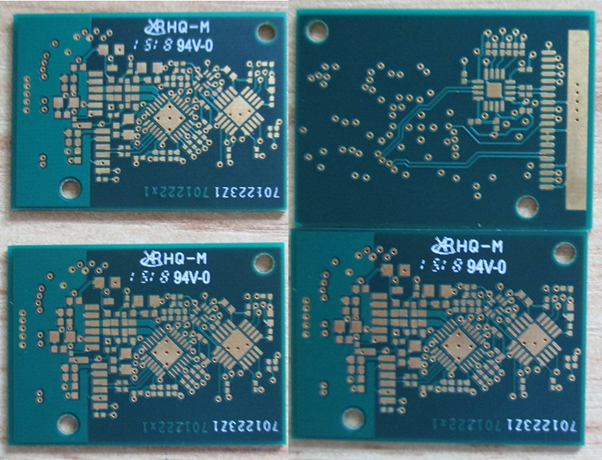
With the trendy information and industry development, the computer circuit board industry is developing rapidly. The copper circuit surface of the computer circuit board is simple to oxidize but has poor solderability. The foremost reliable method is to gold plate the computer circuit board, thus birthing to Gold-Plated PCB. PCBs are the framework of a gold-plated printed circuit that could be a form of PCB with gold plating. PCB gold plating could be a common practice in today’s electronic Industry. Some applications demand the utilization of this PCB thanks to the kind of environment it'll be used. The utilization of gold in plating PCBs is common within the PCB industry. Over time, there is an increase in demand for Gold plated PCBs. PCB gold plating is the process of depositing gold onto the surface of a board through plating.
Hard Gold Surface Finished for PCB
Plating is a very important stage in PCB production. Differing kinds of materials like copper, nickel, tin, and gold. Gold is beneficial for plating circuit boards because of its conductive properties. There is the use of gold contact surfaces on PCBs with membrane switches by experts. Since the gold plating has strong adhesion, it can attach gold particles to the PCBs. Gold plating may be a surface finishing method that uses electrochemical plating to deposit gold onto another metal. Hard gold is extremely durable, so during PCB Fabrication, this finish is sometimes applied to high-wear areas, like edge connector Gold Fingers and keypads, since the hardness of the finish can withstand repeated use; however, thanks to the high cost of hard gold, and its relatively poor solder-ability, it's very rarely applied to solder-able areas.
Gold-Plated PCB is roughly divided into two kinds of gold plating methods and applications. One is terminal plating, which is especially used for products that need frequent insertion and removal of electronic products. For instance, the gold finger plating of adapter cards is typical. This kind of gold plating uses alloy electroplating for surface treatment. The content of gold isn't pure but contains some impurities, to boost the damage resistance of the plating layer.
The foremost drawbacks include being expensive, labor-intensive, use of bus bars and difficulty with other surface finishes therefore the finish doesn't fully encapsulate trace sidewalls, except in finger areas of PCB.
Frequency Oriented PCB
- 1Understanding UL 94V-0 Flammability Rating for Printed Circuit Boards (PCBs)
- 2HDI PCB Market Outlook 2025: Future Prospects, Growth Analysis & Innovations
- 3HDI PCB Design Comprehensive Guide: Mastering High Density Interconnect Technology in 2025
- 4Top 10 Flexible PCB Factories in 2025
- 5Top HDI PCB Manufacturers (2024)
- 6PCB core raw material CCL
- 7IC Substrate | Comprehensive Guide (2021)
- 8How to Make mSAP PCB?
- 9Top 10 IC Substrate Fabricators (2024)
- 10The Impact of Trump's Tariff Policy on Chinese PCB Industry and Countermeasures

- Skype ID: shawnwang2006
- Phone No。: +86-755-23724206
- Email: sales@efpcb.com
- Quick Contact