Transparent PCB Technology Comprehensive Guide (2025)
While electronics design and applications continue to push boundaries as the industry goes on-road with increasingly sophisticated enhancements and capabilities, manufacturing technology and requirements for unique material solutions have never been in higher demand. One of these innovations is transparent PCB technology that revolutionizes engineers' work approach to product development in specific applications where aesthetics, unique form factors and new user interfaces are a must. This in depth guide will lead you through the history, materials used, manufacturing techniques, design hints and more on transparent PCB technology with the most recent industry findings and research pointing sponsorship to industry figures.
What is Transparent PCB?
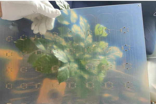
Printed Circuit Board as transparent one is said to be a special type of PCB it contains transparent or semi-transparent substrate and conducting materials that allows you to fabricate lightweight circuit boards for passing through the light. Unlike conventional PCBs that use the fiberglass-reinforced epoxy (FR-4) substrate and copper traces, which are typically opaque; Transparent PCB uses materials like glass, transparent polymers or conductive oxides. This has led to many new possibilities for electronic devices especially in the field of display, wearable electronics, automotive interior screen and advanced lighting technologies.
The Development Trends of Transparent PCB
The idea of a transparent PCB is not something totally new, but commercial readiness speeded up over the recent years due to advances in material science and micro fabrication. According to a 2023 report from MarketsandMarkets, the worldwide transparent PCB market and market for transparent electronics in general will grow to over $2.1B by the end of 2027 driven by increasing consumer electronics as well as automotive and smart home device adoption. Another, the same report also indicates that the transparent PCB technology is appealing particularly in next-generation touch panels, heads-up displays (HUDs) and augmented reality (AR) devices because transparency and electrical performance are most useful.
What is Raw Materials for Transparent PCB?
The technology of transparent PCB starts with the substrate as a foundation. Most commonly used materials are glass, which is exceptionally clear for the air planetary age and has great mechanical strength but also has excellent dielectric qualities. Borosilicate glass, in particular can provide excellent thermal stability and low coefficients of thermal expansion which is an important specifier for high-reliability applications. Polymers, such as transparent polymers like polycarbonates (PC) and polymethyl methacrylate (PMMA) are also used where flexibility or impact resistance are necessities. These materials are specifically designed to provide optimum transparency while maintaining mechanical robustness and process compatibilities.
Most conductive pathways in transparent PCB are fabricated using transparent conductive oxides (TCOs), ITO being the most popular. ITO is one of the best known used materials in transparent conducting applications, as it offers high optical transmittance over the visible spectrum while producing a true electrical resistance. Other emerging materials are graphene, silver nanowires and conductive polymers (such as PEDOT: PSS), each with different unique characteristics in terms of formanability, processability and cost.
How to Make Transparent PCB?
Transparent PCB Fabrication process using (several micro fabrication techniques). Pattern conductive traces employing photolithography, sputtering or inkjet onto transparent substrates is by and large performed way of Photolithography has most common ones used pattern encryption on electrical traces on top of the glass. As in the case of ITO, this is done by sputter deposition which then to patterned with photolithography and masks as well as wet or dry etching. On polymer substrates, screen printing or inkjet printing of silver nanowire pastes or conductive polymers are increasingly used for roll-to-roll manufacturing and flexible electronics. The main issue of Transparent PCB manufacturing concerns to maintain the fine line and defining resolution meanwhile remaining transparent on higher level. The current state of the art for line-width of an ITO-based trans-missive PCB is typically 10 µm and this has been further pushed down to the sub-2 µm range by advances in nano imprint lithography and laser direct writing.
20 microns the use of silver nanowire and graphene inks allows for bendable/or stretchable circuits on flexible Transparent PCBs in the contact line width of about 20 micrometers
Another important aspect to consider is conductive layer bonding on the transparent substrate. If not adhered well, it leads to delamination which is bad for thermal cycling or mechanical vibration. This is often dealt with through bonding optimizers, such as surface treatments like plasma activation or saline coupling agents. Together the protected circuitry is encapsulated with transparent UV resistant polymers for protection against environmental degradation.
Transparent PCB design is an interdisciplinary feature where electrical, optical, and mechanical considerations have to be balanced within the limits imposed by manufacturing. This is to be achieved by ensuring the entire PCB stack has a high enough inlay transmittance for display and touch panel applications of the visible light range ( >90% ), in some cases even more than 95%.
This requires careful consideration of the substrate thickness, conductive layer and thickness also any coatings or adhesives on top. Materials with high UV stability and low yellowing tendencies are preferable in applications where the Transparent PCB is exposed to ambient light or UV radiation.
One of the most important is Signal integrity, especially for high speed or RF circuits. Although ITO and other TCOs have reasonable DC conductivity, their sheet resistance tends to be much larger than copper which leads to signal loss at high frequencies. Systematic design trade-offs (trace width & spacing, layer stack-up) are necessary to achieve optimal performance. In some cases, a hybrid structure that includes transparent and opaque sections is used to balance aesthetics with electrical performance over the array of just the one type.
For example, high power or single-chip power applications for transparent PCB and LED lighting (semi-conductor light bulbs) or automotive displays are some of the biggest Thermal challenge in applications. Glass being inherently very thermally conductive versus polymers, the glass boundary (and thus the inscribed device) must be engineered from the mechanical standpoint. Combining with micro structured heat spreaders and/or transparent thermal interface materials in the “standard” TC piles of the Transparent PCB board to deliver heat efficiently and to leave an optical clear defines the optimal heat-conducive configuration with better heat dissipation efficiency.
Transparent PCB Applications
- Consumer electronics: The transparent PCBs are growing with the maturing of the technology. They are ideal for making bezel-less touch panels, transparent speakers and see-through control interface in consumer electronics such as mobile phones. For example, the next-generation mobile Apple iPhone X uses the OLED display stack to allow finger swipe events and maintains a seemingly borderless design with transparent PCB. In automotive, Transparent PCB is found in heads-up displays (HUDs), smart mirrors and ambient lighting systems enabling both safety & aesthetics.
- Automotive industry: The automotive transparent electronics market, according to IDTechEx the report projects Transparent PCB will be good enabled with growing compound annual growth rate (CAGR) of >15% from 2023 to 2028.
- The other devices: Another promising area on wearable device and smart textiles. The polymer-based transparent PCB provides flexibility, low weight characteristics making them fabric compatible for the docking of clothing suppliers wellness bands clinic medical sensing. Researchers at the University of Cambridge have produced conformable electronics using silver nanowire networks in transparent PCB based stretchable, by demonstrating that the be able to monitor vital signs is more subtle as they do not obstruct vision from either the wearer or experience it. Architectural and interior design procedures use Transparent PCB to illuminate glass panels, interactive windows, and smart partitions. Applications that use the specific combination of transparency, electrical connectivity, and design freedom supplied by Transparent PCB. Dynamic lighting, information screens and gesture control will be integrated into both residential and commercial environments through the integration of Transparent PCBs with LEDs and capacitive touch sensors.
Sustainability of Transparent PCB
Manufacturing of transparent PCB runs within specific industry standards on quality and reliability. Flexible and rigid-flex PCBs, as well as the IPC-6013 standard (a perspective that can be settled for the Transparent PCB qualification alongside with lighting up, adhesion along with environmental durability examination levels). Many of the top manufacturers use automated optical inspection (AOI) and electrical testing as well as accelerated aging tests to enforce uniformity. Transparent PCB assemblies of mission-critical application are subjected to highly accelerated life testing (HALT), thermal shock cycling in order to establish their long term reliability.
In the manufacturing of transparent PCB sustainability is also one of its important consideration. The use of rare metals (i.e. indium in ITO) has raised curiosity over resource scarcity and recyclability. Hence, research in alternate transparent conductors (copper nanowires, carbon nanotubes, and conductive polymers) is getting pushed as well. Recyclable glass substrates and eco-friendly processing techniques for Transparent PCB are being developed by companies like AGC Inc. as well as Corning, for instance to reduce the environmental impact of making more of these.
The World Economic Forum expects that the use of sustainable electronics manufacturing will differentiate leading practices in global supply chains. Since custom and advanced materials have to be exploited to fabricate Transparent PCBs, as well as a higher level of precision in manufacturing; cost-for this matureness structure remains relatively more expensive compared to traditional PCBs. But given that volume will only increase and new materials will be commercialized, the cost differential should get narrower. At its gist, transparent PCB technology is valuable as a means to support product designs that are not possible with standard PCBs and new forms of user experience, as well as integrated functionalities.
Definitely looking forward, the future of transparent PCB technology is bright. Electronic component miniaturization, the advent of flexible and wearables technologies and increased demand for immersed displays are all causing innovation in Transparent PCB material and process. The coming of ultra-thin glass, flexible ceramics and printable transparent conductors is predicted to create new performance levels with increased design freedom. We expect hybrid transparent PCB structures, a blend of 2D and 3D electronics to be the norm in complicated devices.
The next advance is the building of active devices (thin-film transistors, sensors and micro LED) directly onto the PCB itself which is Transparent PCB. Such an integration will enable fully transparent displays, interactive windows and smart surfaces designed where electronics and architecture join. The merging of Transparent PCB with emerging technologies (such as quantum dots, organic electronics and micro electro mechanical systems (MEMS)) will also broaden its scope of applications.
For engineers and designers to be on the cutting-edge of electronic invention, understanding what makes transparent PCB technology tick is necessary. Stakeholders with an understanding of the unique materials and processes at play also learn to access those possibilities and realize new products to stand out more than most in a crowded marketplace. Not just technologically fascinating, transparent PCB is already an interactive freeform space for creativity, performance and sustainability. If powering the future smartphones, changing automotive interiors or creating wonder architecture spaces meaning no use, than Transparent PCB is rewriting the future of electronics in a way that was never possible before.
References:
MarketsandMarkets, “Transparent Electronics Market—Global Forecast to 2027”
IDTechEx, “Automotive Transparent Electronics 2023–2028”
IPC-6013, “Qualification and Performance Specification for Flexible Printed Boards”
Journal of Materials Chemistry C, “Advances in Transparent Conductive Materials for Electronics”
World Economic Forum, “Sustainable Electronics Manufacturing: The Next Frontier”
- 1Understanding UL 94V-0 Flammability Rating for Printed Circuit Boards (PCBs)
- 2HDI PCB Market Outlook 2025: Future Prospects, Growth Analysis & Innovations
- 3HDI PCB Design Comprehensive Guide: Mastering High Density Interconnect Technology in 2025
- 4Top 10 Flexible PCB Factories in 2025
- 5Top HDI PCB Manufacturers (2024)
- 6PCB core raw material CCL
- 7IC Substrate | Comprehensive Guide (2021)
- 8How to Make mSAP PCB?
- 9Top 10 IC Substrate Fabricators (2024)
- 10The Impact of Trump's Tariff Policy on Chinese PCB Industry and Countermeasures

- Skype ID: shawnwang2006
- Phone No。: +86-755-23724206
- Email: sales@efpcb.com
- Quick Contact