Unraveling the Secrets of RF PCB Design: Harnessing the Power of Connectivity
Keywords: RF PCB
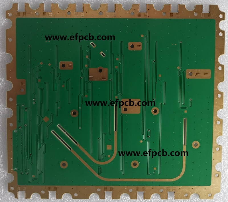
RF PCB is specially engineered circuit boards that are optimized to handle high-frequency signals and minimize signal loss or interference. Unlike regular PCBs, RF PCBs have unique layout guidelines and component placement techniques to ensure optimal performance in transmitting and receiving RF signals. These boards are used in a wide range of applications, including wireless communication systems, radar systems, satellite communication, and medical devices.
Design Considerations for RF PCBs:
Designing an RF PCB requires careful consideration of several critical factors. Here are some important considerations:
- Impedance Matching: Maintaining proper impedance matching throughout the PCB is crucial for minimizing signal reflection and maximizing power transfer. This involves using controlled impedance traces and matching components to ensure the RF signal travels smoothly through the board.
- RF Circuit Layout: The layout of the RF circuit plays a pivotal role in reducing signal loss and interference. RF traces should be kept as short as possible, avoiding sharp bends and crossing traces to minimize parasitic effects. Ground planes and shielding techniques are employed to minimize electromagnetic interference (EMI).
- Component Placement: The placement of components on an RF PCB is critical for signal integrity. RF components, such as antennas, filters, and amplifiers, should be strategically positioned to minimize trace lengths and maintain signal integrity. Proper decoupling of power supply lines is also essential to minimize noise and ensure stable operation.
- Grounding and EMI: RF PCBs require careful attention to grounding techniques. Ground planes are used to provide a low-impedance return path for RF signals and minimize EMI. Separating sensitive analog and digital components on different ground planes helps prevent digital noise from interfering with RF signals.
- Material Selection: Choosing the right PCB material is vital for RF designs. High-frequency laminates with low dielectric constant and loss tangent are preferred to minimize signal loss. Material properties, such as thermal conductivity and coefficient of thermal expansion, also play a role in ensuring the PCB's reliability and performance over a wide temperature range.
- Testing and Validation: Once the RF PCB design is complete, thorough testing and validation are essential to ensure its functionality and performance. Various tests, such as impedance matching verification, signal integrity analysis, and EMI testing, are conducted to validate the design and make necessary adjustments if required.
NEW ARTICLES
- 1Understanding UL 94V-0 Flammability Rating for Printed Circuit Boards (PCBs)
- 2HDI PCB Market Outlook 2025: Future Prospects, Growth Analysis & Innovations
- 3HDI PCB Design Comprehensive Guide: Mastering High Density Interconnect Technology in 2025
- 4Top 10 Flexible PCB Factories in 2025
- 5Top HDI PCB Manufacturers (2024)
- 6PCB core raw material CCL
- 7IC Substrate | Comprehensive Guide (2021)
- 8How to Make mSAP PCB?
- 9Top 10 IC Substrate Fabricators (2024)
- 10The Impact of Trump's Tariff Policy on Chinese PCB Industry and Countermeasures

- Skype ID: shawnwang2006
- Phone No。: +86-755-23724206
- Email: sales@efpcb.com
- Quick Contact