What is HDI PCB
High Density Interconnector PCB (HDI PCB) Summary
HDI is short name for High Density Interconnector. PCB is for Printed circuit board. HDI PCB is high density traces layout within smaller unit area for PCB. So HDI PCB full name is high density interconnector printed circuit board. HDI PCB has been in development for many years. The earliest technology originated in Japan, and began mass production in the 1990s. HDI PCB has become an important branch of PCB, representing the advanced level of the industry today. It is widely used in smart phones, tablet computers, Wifi modules, Bluetooth electronic devices and other high-end electronic products.
HDI PCB development stages:
The first stage, the early stage, from the development of SLC by IBM in 1989 to the mid-1990s, was a period when HDI technology flourished. Various technological processes were being explored, and mainstream HDI technology was not yet available.
In the second stage, from 1995 to 2005, Matsushita Electric and Toshiba respectively successfully developed non-plated hole filling HDI technology, which can realize any layer interconnection; at the same time, laser drilling and HDI technology with RCC/prepreg as the dielectric layer are used in Stand out from the competition and become the most important technical solution.
The third stage, from 2005 to 2010, at this stage, multiple layered technology began to be applied on a large scale, IBIDEN company published FVSS (Free Via Stacked up Structure) in ECWC 10, marking the beginning of HDI into any layer (Anylayer) era.
The fourth stage, from 2010 to present. The epoch-making mobile phone iPhone4 was launched in 2010. This is the first mobile phone to use any layer design with electroplated holes. It marks the beginning of large-scale application of any layer and has become a standard design for high-end mobile phones.
HDI PCB Category:
By PCB processing technology, 1 rank, 2 ranks, 3 ranks, 4 ranks, ect.
Someone made category according to the times of laser drilling, Laser drill once, called 1 rank, Laser drill twice, called 2 ranks, laser drill 3 times, called 3 ranks, ect.
Someone made category according to the times of lamination, laminated once, called 1 rank, laminated twice, called 2 ranks, laminated 3 times, called 3 ranks, ect.
According to surface finish, gold plating HDI PCB, OSP HDI PCB, immersion silver HDI PCB, immersion tin HDI PCB, ect.
HDI PCB Stack up,
Generally, the stack up is 1+N+1, 2+N+2, 3+N+3, 4+N+4, N for non-blind via layers, 1, 2, 3, 4 for number of blind via drilling types. For example, 10L 1+N+1, N is for 8 layers non-blind via from L2-9, 1 is for 1 type blind via, please the the stack up as below, microvia L1-2, L2-9, L9-10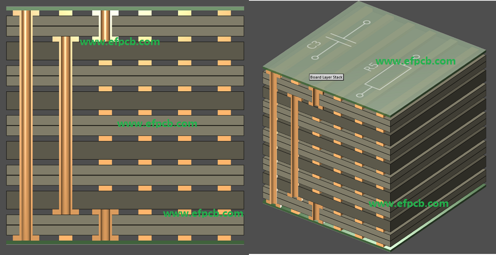
Via in PAD technology
Via in PAD means, via in the PAD, there are 2 processing technologies, one is microvia in PAD, we just use special chemical to plating copper over the vias, and make the PAD flat. The other one is via in PAD, need epoxy plugging, then plating copper over, make the PAD flat.
Application
Cell phone mainboard, computer motherboard, flash memory mainboard, Wifi devices, automotive devices ect.
HDI PCB quick turn service
High Quality PCB is a leading of HDI PCB manufacturer since 1995. up to 5 ranks anylayer HDI projects is available. We can do quick turn service for HDI PCB, 1 rank with 6 working days, 2 ranks with 7 working days, 3 ranks with 8 working days.
What is Flexible PCBs
No More
- 1Understanding UL 94V-0 Flammability Rating for Printed Circuit Boards (PCBs)
- 2Top 10 Flexible PCB Factories in 2025
- 3HDI PCB Market Outlook 2025: Future Prospects, Growth Analysis & Innovations
- 4HDI PCB Design Comprehensive Guide: Mastering High Density Interconnect Technology in 2025
- 5Top HDI PCB Manufacturers (2024)
- 6IC Substrate | Comprehensive Guide (2021)
- 7PCB core raw material CCL
- 8How to Make mSAP PCB?
- 9Top 10 IC Substrate Fabricators (2024)
- 10What is IPC 4761 Type VII Via in Pad PCB?

- Skype ID: shawnwang2006
- Phone No。: +86-755-23724206
- Email: sales@efpcb.com
- Quick Contact