What is IPC 4761 Type VII Via in Pad PCB?
Printed circuit boards (PCBs) are fundamental to electronics in the modern society and the quality of PCBs have a great impact on the performance, reliability, and lifespan of electronics. All these standards are significant for maintaining quality of via in pad PCB designs which are frequently used in high-density / high performance applications, but IPC-4761 type VII is the most vital about it. This post delves into IPC 4761 Type VII and how it corresponds to via in pad PCB technology and the value it adds to PCB manufacturers who follow the standard.
Understanding IPC 4761 Type VII and Via in Pad PCBs
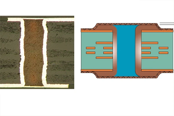
IPC 4761 is a well known industry standard for PCB, as published by IPC (Association Connecting Electronics Industries), which details the design, performance and reliability criteria for vias found on PCBs. Vias are tiny holes made in PCBs to connect different layers of a circuit electrically, allowing even very sophisticated circuits to work reliably. The types described here all utilize filled and capped (filled with conductive or non-conductive material and capped with copper such that the copper is flat with respect to the surface of the dielectric layer the via is formed within) vias, referred to as Type VII vias.
Type VII Vias are especially important in via in pad PCB designs. What is Via in Pad PCB technology Via in pad PCB technology refers to the construction process of putting a via directly in a copper pad that will be ideally occupied by a component lead.ute Designs Running high-speed signals to and from BGAs and flip chips can be tricky with a standard PCB process using dog bones or via in pads. Type VII vias help keep via in pad PCB nice and flat during soldering and prevents solder wicking, as well as facilitate denser designs.
What Is the IPC Standard for Via in PAD PCB?
|
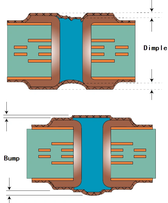
IPC-4671 Type VII for Via in PAD PCB |
|||
|
Items |
Class I |
Class II |
Class III |
|
Capped copper thickness (um) |
AABUS |
5 |
12 |
|
Dimple max (um) |
AABUS |
127 |
76 |
|
Bump max (um) |
AABUS |
50 |
50 |
The standard applicable for via in pad in PCB design are IPC-6012 as well as IPC-4671. IPC-6012 specifies qualification and performance requirements for rigid printed boards, including guidance for microvia design implementation, land pattern design, and electrical characteristics to insure reliability. In contrast, IPC-4671 addresses the performance requirements of printed board laminate materials necessary for vias’ mechanical stability and functionality. These two standards combined offer the complete documentation necessary to develop a viable via in pad PCB in accordance to internationally recognized parameters for quality and reliability.
IPC 4761 Type VII Via in Pad PCB - Key Features
1. Flat Surface for Soldering
Firstly, the most important aspect to via in pad PCB design is to avoid solder from being sucked down the via during assembly. Type VII vias solve this problem by filling the via and capping it with copper, so the surface is level and even for the best soldering and to avoid defects.
2. Enhanced Signal Integrity
High speed, high frequency, signal integrity is key to it. Type VII vias: via-in-pad on PCB designs help to avoid signal distortion and electromagnetic interference (EMI) by eliminating voids and providing a uniform electrical interface.
3. Improved Thermal Conductivity
Cooling is an important issue for high-density and high-power. Type VII vias enhance thermal performance of via in pad PCBs by facilitating heat conduction throughout the board, preventing hot spots.
4. HDI (High Density Interconnect) Design Support
An increasing number of electronics require high-speed and high-frequency circuits and connectors are key elements in them.
Since the use of HDI has to do with reduction of space and higher number of components, it is not surprised that via in pad it is used frequently on HDI designs. Type VII drilling vias permit stacked and staggered formats, they are suitable for HDI applications in aerospace, telecommunication and medical.
5. Mechanical Strength and Reliability
Type VII vias help to build up the via-in-pad PCB by removing voids and adding strength to the via. This makes the resistance of the board to mechanical stresses in assembling and operating it more durable.
Via in Pad PCB Designs Why Use IPC 4761 Type VII?
Compatibility with Advanced Components
With the development from traditional hardware towards the new generation of digital electronic systems, components are becoming smaller, stronger, and smarter. Type VII vias in pad PCB designs With Type VII vias one can take full advantage of fine-pitch components resulting in dense layouts.
Elimination of Solder Voiding
Solder voiding is an issue widely reported in via in pad PCB, which results in poor joints and degraded reliability. Type VII vias prevent voiding by creating solid, planar soldering surface for more robust and reliable bonding.
Improved Manufacturing Yield
Manufacturers can realize increased yields during assembly by meeting IPC 4761 Type VII specification. Type VII via lands make for much easier and simpler soldering processes with less negative effects on yields (costs and time savings in the production process) than other styles.
Compliance with Industry Standards
IPC 4761 Type VII represents the most widely accepted international standard for via in pad PCB designs and guarantees products are developed to the highest standards of performance quality and reliability. This is especially true for sectors that need rigorous quality control, like automotive, aerospace and health care.
Why Our Business Does Well in IPC 4761 Type VII Via in Pad PCB Production
High Quality PCB is a PCB manufacturer that specializes in PCB prototype and also offers low volume and mass PCB production. With modern facilities, experienced engineers and stringent quality systems, we can provide PCBs that are widely used in industrial, communication, instrument and automotive industry. Here’s what sets us apart:
Advanced Manufacturing Capabilities
With the use of the latest in laser drilling, via filling and copper capping, we take pride producing a via in pad PCB with accuracy and uniformity in all of our products. Our facilities accommodate both conductive and non-conductive fills to meet a variety of customer’s requirements.
Expert Engineering Support
We specialise in IPC 4761 standard and via in pad PCBs. We collaborate with customers to state-of-the-art tailored solutions that enable performance, reliability and cost benefits.
Rigorous Testing and Quality Control
All board are 100% e-tested including thermal cycle and solderability test as well as the most sophisticated inspection techniques, AOI and X-ray. This gives compliance with IPC 4761 Type VII and guarantees the reliability of the product.
Global Reach and Industry Experience
We count among our clients a variety of sectors including automotive, telecom, aero-space and consumer electronics with the knowledge and the capabilities to address the specific challenges required by any application. As a trusted PCB manufacturer, we have resources to provide you with high quality & competitive price PCBs.
IPC 4761 Type VII Via in Pad PCB - FAQs
Q1: What is the fill used in Type VII vias in via in pad PCB?
Type VII vias may be filled with conductive materials such as silver or copper paste to provide improved electrical performance and non-conductive materials such as epoxy to provide increased mechanical strength and thermal dissipation.
Q2: Can all Via in pad PCB designs use Type VII vias? Type VII vias are best suited to high-density, high-speed via in pad PCBs, but may be unnecessary in more straightforward designs. Your PCB house will be giving you the optimum via type you should use.
Q3: What is the effect of Type VII vias on Manufacturing Cost?
Complexity in the addition of an additional process step to fill, cap and in turn expose the vias to make them nub free added cost to VIA in Pad PCB printed circuit boards. But the added stability and better performance are usually worth the investment.
Q4: May Type VII vias in via in pad be used?
Type VII vias can definitely be skewed for flexible PCBs-offset, and likely the manufacture process needs added considerations to add bend retention or reliability.
Q5: How are type VII vias in comparison to other via types in via in pad PCB preparation?
Type VII vias vs. Open, Plated, or Filled The driver for Type VII vias is the superior reliability, mechanical integrity and compatibility with the SiP designs of today that they provide. They are favorite in high performance applications.
Wrapping Up With unmatched reliability, signal integrity, and thermal optimization, IPC 4761 Type VII vias are critical to the quality and usability of via in pad PCB layouts. You can always choose a factory focus on this standard, then you can get a PCB board that meets the needs of today’s electronic products with saving cost and guaranteeing quality. If you're designing HDI PCBs, working on thermal challenges, or looking for ways to boost solder reliability Type VII vias are the perfect fit for any application.
- 1Understanding UL 94V-0 Flammability Rating for Printed Circuit Boards (PCBs)
- 2HDI PCB Market Outlook 2025: Future Prospects, Growth Analysis & Innovations
- 3HDI PCB Design Comprehensive Guide: Mastering High Density Interconnect Technology in 2025
- 4Top 10 Flexible PCB Factories in 2025
- 5Top HDI PCB Manufacturers (2024)
- 6PCB core raw material CCL
- 7IC Substrate | Comprehensive Guide (2021)
- 8How to Make mSAP PCB?
- 9Top 10 IC Substrate Fabricators (2024)
- 10The Impact of Trump's Tariff Policy on Chinese PCB Industry and Countermeasures

- Skype ID: shawnwang2006
- Phone No。: +86-755-23724206
- Email: sales@efpcb.com
- Quick Contact