What Is Ultra HDI PCB?
Understanding Ultra HDI PCB
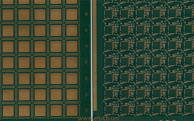
Ultra HDI PCBs are valued for the high wiring density they offer, which facilitates more components to be installed in a smaller region than standard PCBs. This is realized through state-of-the-art manufacturing, which can include such methods as microvias, blind and buried vias, and fine etching. Because the electronic instruments have shrunk in size and become more and more complicated, there is a soaring demand in Ultra HDI PCB, and the Ultra HDI PCB has become the vital part of telecommunications, consumer electronics and aerospace, and so on.
Ultra HDI PCBs Key Features
- Microvias: Ultra HDI PCBs will have microvias which small vias that connected the different layers of the PCB. These microvias can have a diameter as small as 0.1 mm so that the connections can be made very densely packed and the PCB size can be minimized.
- Blind and Buried Vias: With these vias, the connection between layers is not fully through the PCB. The outer layer is connected to one or more inner layers with blind vias, and the inner layers are connected with only buried vias for still greater space savings on the PCB.
- Number of Layer: Ultra HDI PCBs could have many layers, more than 10, can make complex circuits and functions in a small space.
- Advanced materials: Materials available for Ultra HDI PCB manufacturing are usually not the same as FR-4, but can be specialty materials that are better suited for high-frequency applications or for better thermal performance. Such materials are low-loss dielectrics, and high-temperature substrates.
Ultra HDI PCBs Manufacturing Process
Ultra HDI PCBs production process features quite a few complex steps, and all are planned to deliver precision and quality. Here is a closer look at the usual order of events:
1. Design and Layout
It all starts in the design process where engineers employ powerful software to design the PCB layout. At this point, we are identifying the location of parts, the routing of traces, and establishing a stack-up. The layout has to make it easy for the design to consider the large number of connections and the layout must take the electrical/mechanical requirements into consideration.
2. Material Selection
The selection of materials is fundamental to Ultra HDI PCB performance. Commonly used materials include FR-4 for normal applications, Isola and Tuc for multilayer, and Rogers or PTFE for high-frequency circuit boards. Dielectric The type of dielectric material significantly impacts the performance of the PCB with respects to its signal integrity as well as its thermal characteristics.
3. Imaging and Etching
After the layout is completed, the PCB is ready to be imaged. A photosensitive film is deposited on the copper clad substrate, and the design is replicated on the film with the aid of ultra violet light (UV light). Following this exposure, the board is developed and undesired copper is then etched away to create the circuit pattern.
4. Via Formation
The microvias is the key technology of Ultra HDI board. This may be accomplished by laser drilling which provides for precise size and location of the vias. The vias are drilled and copper is plated in to form conductive traces.
5. Layer Stacking and Bonding
In case of multi-layer Ultra HDI PCBs, layers are aligned and attached by up to two prepreg materials. These isolated layers are then subjected to heat and pressure in a lamination step that unites them and cures the prepreg to form a solid structure.
6. Surface Finishing
In the last step the surface is finished, so that this soldered pad is protected from the environment and has good solderability. Typical finish types include HASL (Hot Air Solder Level), ENIG (Electroless Nickel Immersion Gold) or OSP (Organic Solderability Preservative).
Advantages of Ultra HDI PCBs
Ultra HDI PCBs vs. traditional PCBs There are several benefits to using an ultra HDI PCB over a traditional PCB, making it an ideal choice for manufacturers:
- Small Footprint: High density of connections translates to less PCB area which is perfect for portable and space limited applications.
- Better Performance: Signal integrity and thermal performance are improved with the latest composite materials and connection technology for high frequency applications.
- Higher Performance: With more parts fit into a smaller space, Ultra HDI PCBs allow for creating more complex electronics without the need for increased size.
- Costs: Although ‘per job’ costs can potentially be higher after the startup costs, the reduction in downtime keeps the overall product production costs lower in jobs manufactured in large lots.
Applications of Ultra HDI PCBs
Ultra HDI technology PCB has the advantages of high performance, high reliability, etc. and is widely used in many application fields. Some notable applications include:
Consumer Electronics: Products like smart phones, tablets and wearables take advantage of the small footprint and high performance of Ultra HDI PCBs.
Telecom: Network equipment and communication devices need high speed PCB to ensure effective data transport through itself.
Aerospace/Military: The high integrity and robustness of Ultra HDI PCBs make them perfect for mission-critical elements in the flight and military hardware.
Automotive The more and more electronic vehicles are, the more and more UHDI PCB plays a key role in the advanced systems such as ADAS and infotainment systems.
Frequently Asked Questions (FAQ) about Ultra HDI PCBs
How do HDI PCBs differ from the Ultra HDI PCBs?
(HDI) printed circuit boards usually have lower number of interconnections compared to Ultra HDI PCBs. Microvia and blind via enable the use of Micro technology which has higher HDI microvia technology HDI density than traditional printed circuit boards.
Is Ultra HDI PCB costlier to produce?
Yes, manufacturing Ultra HDI PCBs is more complicated and involves using special facilities and equipment and thus may be more expensive. But the gains are usually well worth it in performance and functionality gains.
Can Ultra HDI PCBs applied in the field of high frequence?
Absolutely. The high-end materials and advanced design technology introduce in the Ultra HDI PCBs is perfect for high-frequency applications by support signal integrity and low loss.
How can I select the best manufacturer for Ultra HDI PCB?
When choosing a maker, their experience with Ultra HDI technology, reliability certs and capability of satisfying your particular board style must be taken into consideration. It’s also best to check their past work and customer reviews.
Which industries gains the most from Ultra HDI PCBs?
What industries benefit the most from ultra HDI PCB technology The following industries, among many others, benefit from Ultra HDI PCB technology due to the advantages it provides high performance applications, including: Consumer electronics Telecommunications Aerospace Automotive Medical devices.
Conclusion
Ultra HDI PCBs are a giant step in PCB technology, providing density, performance, and functionality unimaginable just few years ago. As high-tech devices advance, the significance of Ultra HDI PCBs will increase and the position of UHDI boards as a mainstream technology in electronic manufacturing will be reinforced.
- 1Understanding UL 94V-0 Flammability Rating for Printed Circuit Boards (PCBs)
- 2HDI PCB Market Outlook 2025: Future Prospects, Growth Analysis & Innovations
- 3HDI PCB Design Comprehensive Guide: Mastering High Density Interconnect Technology in 2025
- 4Top 10 Flexible PCB Factories in 2025
- 5Top HDI PCB Manufacturers (2024)
- 6PCB core raw material CCL
- 7IC Substrate | Comprehensive Guide (2021)
- 8How to Make mSAP PCB?
- 9Top 10 IC Substrate Fabricators (2024)
- 10The Impact of Trump's Tariff Policy on Chinese PCB Industry and Countermeasures

- Skype ID: shawnwang2006
- Phone No。: +86-755-23724206
- Email: sales@efpcb.com
- Quick Contact