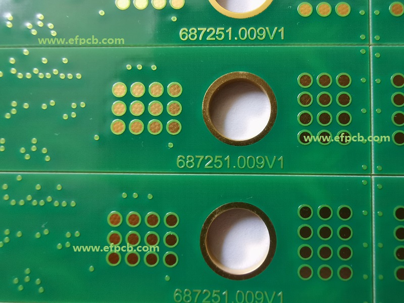
What Is Via in PAD PCB?
A via in PAD PCB, also known as “Via-on-PAD PCB”, is a PCB that has vias that are located / positioned directly within the solder pad of a component. This is used often with high-density PCB layouts, particularly if the component is fine-pitch (BGA etc.) or has a small footprint. The objective of Via-in-Pad is to save space, improve electrical performance and simplifying routing in small pitch packages. Nevertheless this method requires attention to process control during manufacturing because of the risk that, for example, solder will flow into via and that in turn leads to soldering errors. To solve these problems processes, such as via plugging or filling with conducting or non-conducting material subsequently planarization, are widely used by the manufacturers. Correct processing of Via-in-Pad is a prerequisite for reliable functioning and enables the miniaturization of electronic equipment.
Why do we require passes Via in PAD PCB?
Using Via in PAD is not avoidable due to optimization and decreasing of the time of designing the PCB. With vias placed on the PAD directly, the proposed method not only makes a better use of the available space but also it attenuates the crosstalk that appears that results in a better electrical behavior, especially for the high-density and high-frequency designs. It also facilitates routing by eliminating the burden of extra layers, or difficult via structures, lowering the cost of production and number of design iterations. Via in PAD PCB is a key technology enabler for realizing small, reliable and high performance PCB layouts in today's electronic applications.
How to Make Via in PAD PCB?
Generating via in PAD PCB also introduces a very refined procedure of electrical connection and solid connection. First you need to set up your design in your PCB layout package so that it knows where about on your board you want to have vias, the type of vias you want to use and how big they should be (i.e. tell your PCB manufacturer what you like to have). Make sure to have via in PAD where they will connected to. After that, select the hole size and final finish according to the current-carrying capability and signal need. The PCB is drilled in the place where the vias are desired, and the holes are plated with conductive material (usually copper) to connect all the layers. Design rules such as spacing and annular rings must be obeyed to prevent shorting or manufacturing issue. Finally, validate by means of functionality through test and inspection to the desired design requirements and performance.
What Is the IPC Standard for Via in PAD PCB?
|
Items |
Class I |
Class II |
Class III |
|
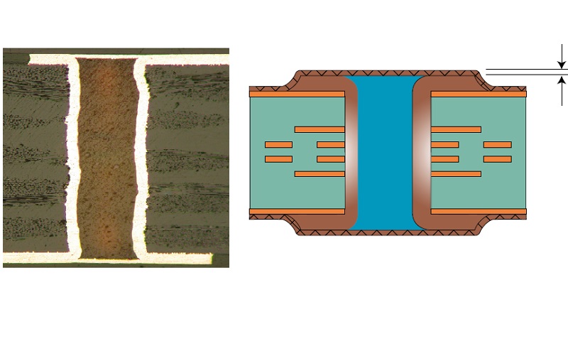
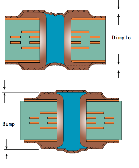
Capped copper thickness (um) |
AABUS |
5 |
12 |
|
Dimple max (um) |
AABUS |
127 |
76 |
|
Bump max (um) |
AABUS |
50 |
50 |
The IPC standards that apply to via in pad in PCB design are IPC-6012 and IPC-4671. IPC-6012 describes the qualification and performance requirements for rigid printed boards, its gives guidance in the areas of via design, selection of land pattern, and guidelines of manufacturing tolerances to ensure that high reliability is maintained in the product. Contrarily, IPC-4671 addresses the performance requirements for printed board laminate materials, which are crucial to mechanical stability and functionality of the holes (vias). Combined, these two standards offer full document coverage to help ensure successful vias in pad PCBs are made, based on industry-recognized quality and reliability goals.
To sum up, using via in PAD PCB layout would be a good way to get best use of space and better electrical capability, especially in some high-density and multilayer boards. However, such an approach needed a due attention on the solderability; thermal management; and potential reliability concerns. Good design practices, such as solder mask defined pads, proper sized vias, good clearance, are necessary to avoid problems like solder wicking and voids during assembly. Collaboration with fabrications and following fab rules are essential in obtaining a successful via in PAD implementation, thus preserving PCB integrity and operability.
What Is Ultra HDI PCB?
- 1Understanding UL 94V-0 Flammability Rating for Printed Circuit Boards (PCBs)
- 2HDI PCB Market Outlook 2025: Future Prospects, Growth Analysis & Innovations
- 3HDI PCB Design Comprehensive Guide: Mastering High Density Interconnect Technology in 2025
- 4Top 10 Flexible PCB Factories in 2025
- 5Top HDI PCB Manufacturers (2024)
- 6PCB core raw material CCL
- 7IC Substrate | Comprehensive Guide (2021)
- 8How to Make mSAP PCB?
- 9Top 10 IC Substrate Fabricators (2024)
- 10The Impact of Trump's Tariff Policy on Chinese PCB Industry and Countermeasures

- Skype ID: shawnwang2006
- Phone No。: +86-755-23724206
- Email: sales@efpcb.com
- Quick Contact