HDI PCB Design Comprehensive Guide: Mastering High Density Interconnect Technology in 2025
High Density Interconnect (HDI) printed circuit boards are at the forefront of contemporary electronics manufacturing, enabling next generation very small form factors and high performance devices. As consumer electronics further miniaturize with increasing functionality, HDI PCB design is now a requirement for engineers designing applications in smartphones, tablets, wearables and high- end computing systems.
According to MarketsandMarkets research, the worldwide HDI PCB market stood at $16.2 billion in 2024 and is projected to grow to $24.8 billion by 2029. This meteoric increase is indicative of how important HDI PCB design is becoming in advanced electronics, as ever-shrinking PCB real estate and increasing performance demands stretch traditional PCB technologies to the breaking point.
Understanding HDI PCB Technology Fundamentals
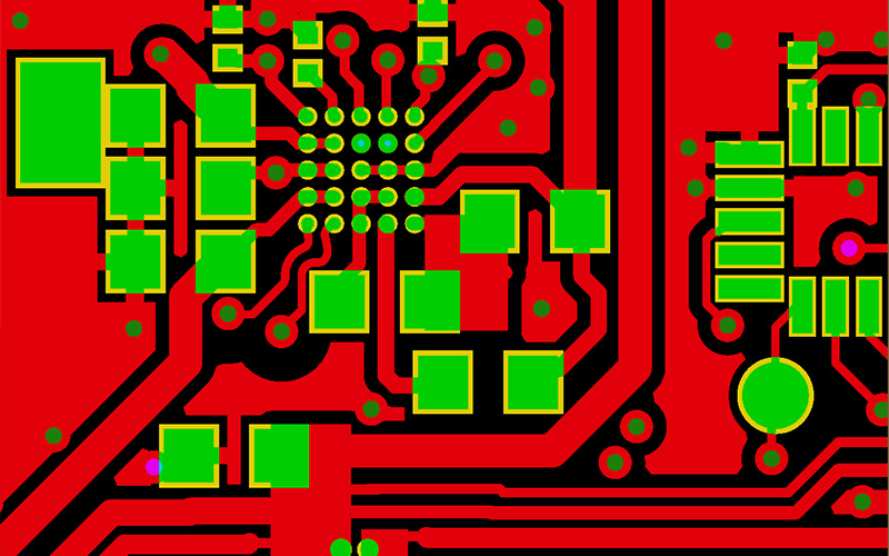
HDI PCB design greatly varies from traditional PCB design with its application of microvias, buried vias, and blind vias for higher circuit density. The boards typically have trace widths of 25 micrometers and via diameters of 50 micrometers, as opposed to in conventional PCBs 100 micrometer traces and 200 micrometer vias are rare.
The process allows designers to cram more horsepower into tighter footprints by using multiple build-up layers on both sides of the core substrate. Now it's possible to design a 20 layer HDI PCB with a thickness similar to that of a standard 8 layer PCB. Such density enhancements are made possible through new materials such as modified epoxy resins, and polyimide films with outstanding electrical characteristics and thermal stability.
Typical defining features of HDI PCB design include via-in-pad technology, which enables components to fight over the counter to be placed directly over vias, and sequential build-up construction in which different layers are added incrementally instead of at once. These capabilities allow routing densities well in excess of 130 connections per square inch as opposed to 50-70 connections of other types.
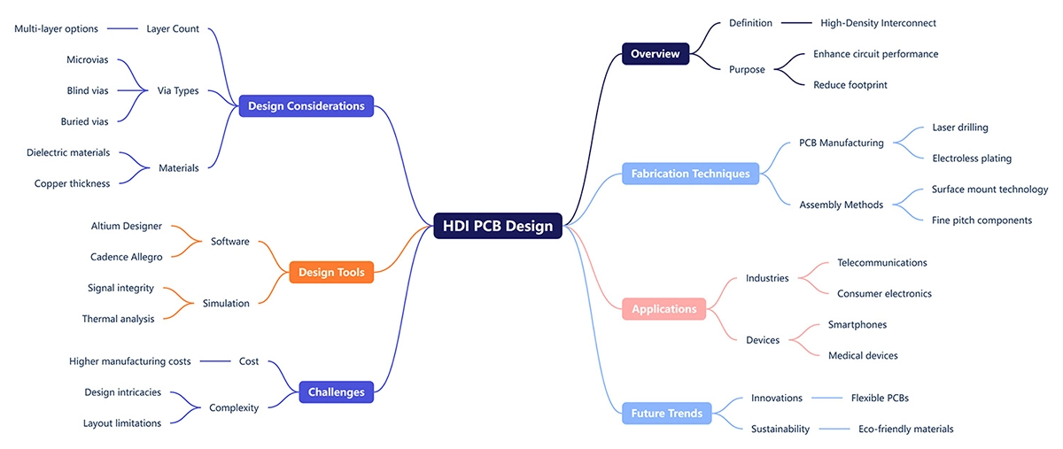
The Manufacturing Technology Process for HDI PCBs
The production of HDI PCB design includes advanced sequential buildup technology, the control of every detail is essential. This flow is important for designers to tailor their layouts for high yield and reliability.
Substrate Preparation and Core Processing
The process starts with preparation of an excellent quality core material which has been developed specifically for HDI applications. The substrate material is usually low-loss dielectric, which controlled dielectric constant ranging from 3.2 to 4.5. In case of using high-end HDI PCB design, substrates including embedded components or cavities can be used to enhance component density. The main processing consists of drilling, plating and patterning the base layers with assembly procedures similar fine with fine techniques used in PCB. With HDI PCB, however, the tolerances need to be much stricter, with a drill tolerance of ±12.5 microns and a copper thickness tolerance across the panel of ±10%. These ranges assure the formation of reliable vias in subsequent build-up levels.
Sequential Build-Up Layer Construction
And when it comes to HDI PCB manufacturing, the heart of the process is the sequential lamination buildup through the addition of layers, one by one. In each build-up layer, prepreg materials which are usually 3-5 mil thickness. They are used to be laid down and then copper foil lamination is performed with predetermined temperature and pressure.
Temperatures during lamination operations are generally between 130 and 260° C and pressures of between 300 to 400 PSI are maintained. The curing must be carefully controlled to avoid delamination and to obtain good bonding between layers. Vacuum-Assisted lamination which ensures void free and uniform layer thickness in modern HDI PCB manufacturing.
Microvia Formation Technologies
Among various difficulties in the fabrication of HDI PCB, microvia drilling is one of the most crucial. There are three major technologies that control this process: laser drilling, mechanical drilling, and plasma etching. Laser drilling with CO2 or UV lasers is responsible for 85% of microvia creation in HDI PCB design arenas.
CO2 laser drilling in the ultrared frequencies of approximately 10.6 micrometer is utilized to ablate organics, such as the dielectric layers, but leave the copper layers unaltered. This selectivity permits accurate depths of blind vias, which bond by certain pairs of layers. UV lasers at 355 nanometers provide sub-75-micron via performance opportunities.
Optimization of laser drilling process needs careful parameter adjustment of pulse energy, repetition rate, and beam focus. Standard parameters for HDI PCB applications are pulse energies between 0.1-0.5mJ at repetition rates of 1-10kHz. These conditions are realized by formation rates of 200-500 holes per second and accuracy of hole size within ±5 microns.
Metallization and Plating Processes
After via formation, HDI PCB design manufacturing requires special metallization techniques to provide stable electrical connections. Treatments such as permanganate solutions or plasma for desmearing, to remove the resin from via walls and enhance copper adhesion.
Deposition of the initial conductive layer, usually 0.2 to 0. 5µm, and an electrolytic copper plating to have a final thickness of 15 to 25µm. The plating also has to offer consistent distribution of thickness between all via sizes and aspect ratios, these varying widely in HDI PCB design uses.
Filled Vias – A lot or a little? Modern HDI PCB design often utilizes filled vias with conductive or non-conductive materials. Conductive filling employs copper paste or high silver-filled epoxy, while non-conductive filling uses special resins that could be planed for further processing. This construction allows for (VIP) via-in-pad construction and enhanced thermal management on high power systems.
Pattern Formation and Etching
In HDI PCB design, circuit pattern forming need a high level of photolithography tool which can create fine-line geometries. Typically dry film photoresist with 15-40 micrometer thickness is employed, depending on copper thickness and line width required.
Resolution capabilities of the exposure systems should be 10 micrometers or less and the alignment accuracy between tiers must be +5 micrometers. Process of HDI PCB design, manufacturing today, the PCB industry benefits from direct imaging systems, which do not require photo masks and lead to greater precision and faster production.
Unwanted copper is removed during etch while desired circuit patterns are protected. Alkaline etchants, usually cupric chloride or ferric chloride, are employed at controlled temperature, concentration and spray pressure. Etch rates need to be optimally adjusted in order to ensure the uniformity of the line width control as well as to keep the undercut to a minimum.
Surface Finishing and Final Processing
HDI PCB manufacturing ends with surface finishing treatments which serve to protect the exposed copper and make soldering possible. Common finishes are Electroless Nickel Immersion Gold (ENIG), Immersion Silver, and Organic Solderability Preservative (OSP).
The gold CSC attains a thickness of between 0.05 and 0.2 mu m on approximately 3-6 mu m of nickel by ENIG, the finishing process which is most suitable for fine pitch applications. This lead finish has a good solderability and wire bondability, and is resistant to storage. The process involves the maintenance of bath chemistry and temperature with fine control to eliminate black pad defects, which can reduce joint reliability.
After final processing, units are then electrically tested with flying probe or bed-of-nails fixtures capable of reaching the very dense test point count typical of HDI PCB versus package design style. AOI system shall confirm maximum and minimum dimensions and defects that may cause failure in the assembly.
Quality Control and Testing Protocols
High density interconnector PCB layout production requires strict quality control in the production process. Statistical process control is used to monitor such critical parameters as via size distribution, copper thickness and uniformity, and dimensions. Typical control limits do not allow via diameter to vary more than ± 10% from nominal, or the copper weight is ±15%.
HDI PCB design reliability test protocols are thermal cycling, vibration testing, and accelerated aging with controlled temperature and humidity. These tests confirm that the sequential build-up process can tolerate those stresses experienced in end-use applications.
Future Trends and Innovations
The HDI design is further progressing with innovations like embedded component technology, 3D printing of conductive traces and advanced materials with superior thermal and electrical properties. These developments indicate that Miniaturization and Functionalization of electronics is poised to reach new heights.
According to industry study there will be artificial intelligence equipped in next-generation HDI PCB to achieve automatic routing optimization and predictive quality control. These advances will continue to enhance manufacturing efficiency while introducing new levels of circuit packing density and performance.
Frequently Asked Questions for HDI PCB Design
What is the smallest VIA that can be achieved in HDI PCB design today?
The smallest wholediameter acceptable is currently about 50 (and in some specialized process, 25) micrometers. However 75-100 micrometer vias are more typical in a production HDI PCB design for reliability and yield reasons.
What is a maximum in HDI PCB design regarding build-up layers?
Today, HDI PCB design supports up to 6 layers build-up on each side of the core, which results to boards having 20+ layers in total. However, 2-4 layers of build-up per side are employed in most commercial applications to compromise the cost and complexity.
What does HDI PCB design cost versus a regular PCB?
HDI PCB design ususally is about 2-5 times higher than similar conventional PCB boards as the acquirement of specific raw materials and use of particular equipment. But the added cost is often traded against lower assembly cost and better product performance.
What are the rules of design to follow for HDI PCB design is that successful?
Key design rules are a minimum trace width of 50 μm, a minimum via spacing of 100 μm and the avoidance of acute angles in the film circuit lines. Signal Inteegrity – The stackup and impedance control is also just as critical.
How is the thermal design affected by HDI PCB design?
HDI PCB designs can help with thermal management by using higher concentrations of copper as well as thermal vias. But the presence of thin dielectric layers and high component density can also lead to thermal issues and should be accounted for in the thermal modeling and optimization of layouts.
Well-mastered HDI PCB design manufacturing technology is a very important competitive edge in the electronics industry today. With devices requiring more and more features in smaller products, knowledge of these advanced manufacturing steps are critical for successful product development and market leadership.
No More
- 1Understanding UL 94V-0 Flammability Rating for Printed Circuit Boards (PCBs)
- 2HDI PCB Market Outlook 2025: Future Prospects, Growth Analysis & Innovations
- 3HDI PCB Design Comprehensive Guide: Mastering High Density Interconnect Technology in 2025
- 4Top 10 Flexible PCB Factories in 2025
- 5Top HDI PCB Manufacturers (2024)
- 6PCB core raw material CCL
- 7IC Substrate | Comprehensive Guide (2021)
- 8How to Make mSAP PCB?
- 9Top 10 IC Substrate Fabricators (2024)
- 10The Impact of Trump's Tariff Policy on Chinese PCB Industry and Countermeasures

- Skype ID: shawnwang2006
- Phone No。: +86-755-23724206
- Email: sales@efpcb.com
- Quick Contact