HDI PCB Market Outlook 2025: Future Prospects, Growth Analysis & Innovations
The global high density interconnect (HDI) market is witnessing robust growth as a result of the burgeoning demand for miniaturized and high-performance electronic devices, which is propelling the market towards becoming one of the fastest-growing sectors of the printed circuit board (PCB) industry. High-Density Interconnect (HDI) PCBs can be designed with finer lines, smaller vias and higher wiring density. Considering the rapid evolution of communication, automotive, consumer electronic and other industries, the HDI PCB market is anticipated to grow exponentially in 2025.
In this article, we will discuss the HDI PCB market 2025 along with the key trends, drivers and challenges, and how our company’s inventive HDI PCB solutions are transforming the future of this ever-evolving industry.
What Are HDI PCBs?
High-Density Interconnect (HDI) PCBs are sophisticated circuit boards in which the density of the wiring per unit area is high. They employ microvias, blind and buried vias, fine trace routing and other technologies that allow more components to be packed into a smaller area. HDI PCBs are also extensively used in fields where size, weight and performance are paramount, including mobile phones, wearable technology, automotive and medical devices. As electronic products shrink and become more complex, the HDI industry has developed to be a pivotal provider of innovation with capabilities for greater design complexity and increased electrical performance.
Factors Influencing Expansion of HDI Market
Growing Importance for Smaller Size
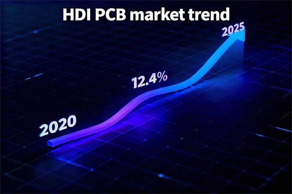
Miniaturization trends across the world is a positive sign for the HDI PCB Market. Today’s devices — whether smartphones or IoT sensors — need smaller, more efficient PCBs to enable advanced features while fitting inside an ever smaller form factor. The high density interconnect printed circuit board (HDI PCB) market is expected to witness a compound annual growth rate (CAGR) of 12.4% from 2020 to 2025, due to manner of increasing usage of compact electronic products, says the report by Mordor Intelligence.
Booming of 5G Technology
The introduction of 5G networks is also driving the HDI PCB market. PCBs for 5G-based products need to support higher frequencies, transmit data faster, and have lower latency. HDI PCBs are crucial for the design of 5G smartphones, base stations, New Radio (NR) network infrastructure and much more, as they deliver superior signal integrity and high-frequency performance.
Growth in Automotive Electronics
The automotive industry is experiencing a technological evolution, including electric vehicles (EVs), autonomous driving, and advanced driver-assistance systems (ADAS). These innovations require high performance PCBs to accommodate the complexity of circuits and working environment. The automotive sector is the growing area of HDI PCBs as in high speed data processing, high density, small, compact packaging and in applicable solutions.
Developments in Technology for Wearables
The HDI PCB market is being powered by the penetration of wearable devices, including smart watches, fitness bands, and medical sensors. These products are extremely high volume and require very high density of wiring, with multiple layers and advanced technologies like buried vias and blind vias to integrate many functionalities including sensors, processors and wireless communications in small form factors.
Technological Innovations in Portable Battery Chargers
The development of manufacturing processes, including laser drilling and modified semi-additive processing (mSAP), enables HDIs with smaller line widths, line spaces, and drilled holes as well as higher numbers of layers. The inventions are slowly enabling production at a lower cost and better quality HDI PCBs, which is driving growth in the HDI PCB market.
Problems in HDI PCB market
Although the HDI PCB market is predicted to offer enormous potential for growth, it is not without some challenges, including:
- High Production Costs: Complex HDI PCB production processes such as laser drilling and mSAP entail substantial capital outlay.
- Intricate Design Considerations: HDI PCB designs require skill and accuracy, a simple mistake can affect the function or reliability of the product. Material Limitations: The production schedules and costs can be influenced by the accessibility of the quality materials, such as low-loss dielectrics and high-temperature substrates.
High Quality PCB has created unique solutions to these issues and now we are still the HDI PCB market leader.
Our Company's Role in HDI PCB market
Being one of the best advanced PCB manufacturers, our company always provides the most advanced HDI PCBs to our customers to will the diversified demands. Here’s what makes us unique in the HDI market:
Advanced Manufacturing Capabilities
In mSAP PCBs, we also have advanced manufacturing capabilities like laser drilling to support the finest lines, microvias, and high layer counts in producing HDI PCBs. We have advanced technology to provide you with high wiring density, high performance pcbs stfying next generation electronics.
Customization and Flexibility
Every project is unique, and we are proud to provide fully personalized HDI PCB solutions. For high frequency 5G device or tiny automotive system, we assist customer to create PCBs that fit their unique requirements. Quality, plushness of detail, and certainty are the values.
Quality is at the heart of everything we do. Our HDI PCBs are tested, audited, and inspected during manufacturing to guarantee that they comply with IPC-6012 and ISO 9001 industry standard. This dedication to quality has won us the confidence of the top OEMs and Tier 1 providers in the HDI industry.
Sustainability Initiatives
We are committed to sustainability by utilizing green materials and sustainable manufacturing. By utilizing our products clients can meet their performance needs and reduce environmental impact.
Outlook for the HDI PCB market
The HDI PCB market is anticipated to experience substantial growth in the subsequent years, owing to the technological innovations and growing applications in multiple industries. Here are a few of the highlights:
- Growth of 5G Networks: Demand for high performance HDI PCBs will increase as 5G adoption grows.
- Growth in IoT and Wearables: The expanding presence of IoT devices and wherable technology will increase opportunities for HDI PCBs in small, high end applications.
- Introduction of New Materials: Advanced materials, such as low-loss dielectrics and high thermal conductivity substrates, will revolutionize the capabilities of HDI PCBs. Our company is able to take full advantage of these trends due to our priorities of innovation, quality and customer satisfaction.
Conclusion
The HDI PCB market is predicted to be a vital factor in the future of electronics with offering are best in size, performance, and reliability. As a pioneer in this domain, we strive to cater to the changing requirements of our customers by offering innovative HDI PCB solutions.
Applying backend of line (BEOL) processes for assembly and interconnection of chips to achieve advanced chip integration and the HDI manufacturing technology, both based on advanced technology, we are pleased to be forging the future of the HDI PCB market with strong commitment to high-precision manufacturing, customization, and sustainability Intentions are expressed. If you are designing the next generation smartphones, automotive systems, or IoT devices, our expertise and state of the art technologies make sure your product will stand out in the market.
Get in touch with us today for more information about our products and services, and how we can assist you in staying ahead in the fast paced environment that is HDI PCBs.
- 1Understanding UL 94V-0 Flammability Rating for Printed Circuit Boards (PCBs)
- 2HDI PCB Market Outlook 2025: Future Prospects, Growth Analysis & Innovations
- 3HDI PCB Design Comprehensive Guide: Mastering High Density Interconnect Technology in 2025
- 4Top 10 Flexible PCB Factories in 2025
- 5Top HDI PCB Manufacturers (2024)
- 6IC Substrate | Comprehensive Guide (2021)
- 7PCB core raw material CCL
- 8Top 10 IC Substrate Fabricators (2024)
- 9How to Make mSAP PCB?
- 10The Impact of Trump's Tariff Policy on Chinese PCB Industry and Countermeasures

- Skype ID: shawnwang2006
- Phone No。: +86-755-23724206
- Email: sales@efpcb.com
- Quick Contact