Stack-Up Strategies for HDI PCB Design
The technology of High Density Interconnect, or HDI, is the backbone of the modern-day PCB. It is the enabling factor that answers the impossible double demand of even higher performance and of even greater miniaturization. And of the many aspects of a successful HDI implementation, we’ll be taking a look today at the stack-up, or the rational organization of conductive and dielectric layers, and one of the most critical parts of the multi-faceted design process that is PCB design. We shall explore strategies, and review the most important aspects that you will be considering when designing your HDI PCB.
HDI PCB Stack Up
The stack up of an HDI PCB refers to the intelligent arrangement of the layers of copper, prepreg, and dielectrics in ways to maximize wiring density and electrical performance. HDI PCB stack-ups will be dealing with several additional considerations in addition to all of the considerations that HDI shares with conventional PCBs: microvias, finer lines, thinner dielectrics, all of which are necessary conditions to the compact and high-performance quality of which HDI boasts.
Of the many components of an HDI PCB stack-up, the core provides mechanical stability, and the prepreg bonds layers together. Thinner copper and dielectrics are often used to support additional layers and finer traces. A well-designed stack-up will help with electrical performance on the end product, manufacturability for your supplier, as well as the cost.
Types of HDI PCB Stack Ups
The types of stack-ups are categorized according to the arrangement and the number of layers laminated around the core. The main types that you’ll be encountering are:
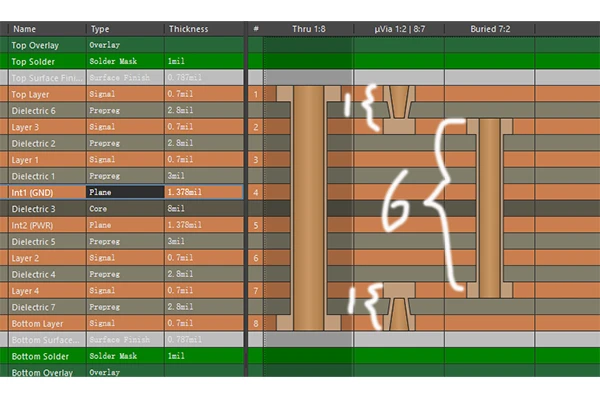
- 1 + N + 1: a single HDI layer both on top of and below a core with N inner layers. The flollowing picture is for 1+N+1 HDI PCB stack up, "N" is 6 layers, "1" is 1 rank HDI or once laser microvia.
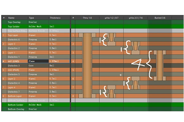
- 2 + N + 2 and 3 + N + 3: multiple HDI layers sequentially laminated. This type of stack-up supports higher routing density for products with demanding signal and pin-count requirements. The flollowing picture is for 2+N+2 HDI PCB stack up, "N" is 4 layers, "2" is 2 ranks HDI or twice laser microvias.
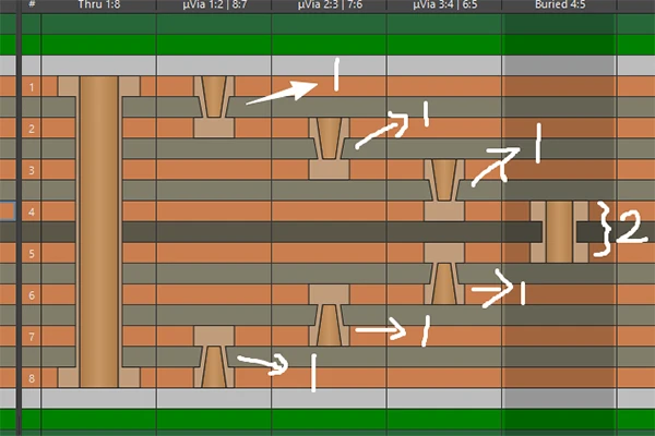
- The flollowing picture is for 3+N+3 HDI PCB stack up, "N" is 2 layers, "3" is 3 ranks HDI or 3 times laser microvias.
- Any-Layer HDI: microvias connect any two layers, offering maximum design flexibility as well as maximum density. This is the type used in high-end consumer electronics.
The choice of the correct type of stack-up will depend on the complexity of your design, on your signal requirements, and on the capabilities of your manufacturer.
Microvia Implementation Strategies for HDI PCB
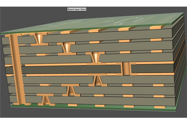
Microvias are a defining characteristic of HDI PCB. You will be seeing two very different figures:
- Staggered Microvias: microvias offset between layers like a flight of stairs. This design distributes mechanical stress, and in this way improves long-term reliability.
- Stacked Microvias: microvias placed directly on top of one another in the manner of an elevator shaft. Vertical density is maximized, but on the conditions of advanced copper filling and precise process control.
Copper-filled microvias will be able to prevent collapse during reflow soldering and maintain electrical performance. Your design team will want to observe recommended HDI aspect ratios and depth limitations for a consistent manufacturing yield.
Signal Integrity
Signal integrity is another one of the key considerations to your HDI PCB stack-up. You want your stackup to maintain careful impedance control, layer sequencing and noise mitigation:
- For impedance control, place signal layers adjacent to reference planes and control dielectric thickness. These arrangements are essential for stable transmission line impedance.
- Dense routing in HDI PCB stack-ups causes signal coupling. This phenomenon known as crosstalk can be mitigated by strategic ground shielding and spacing as well as an intelligent layer order.
- Tackle the problems of electromagnetic interference and signal degradation with proper return path placement.
Thermal and Power Distributions for HDI PCB
As the density of a device increases, thermal management and power distribution will become more and more of a problem:
- Dedicated power and ground planes can lower impedance and ensure robust current delivery. This is especially important in projects with high-performance components.
- The density of an HDI PCB stack up will end up trapping heat. A good design should use thermal vias and via-in-pad structures to channel heat away from critical areas.
- A via-in-pad structure can create direct thermal and electrical connections but will require void-free filling and capping processes.
These considerations will be vital for both the reliability and the longevity of your HDI PCB project.
Material Choices for HDI PCBs
- High-Tg Laminates are good for HDI boards that will be experiencing higher temperatures or multiple reflows.
- Low-Loss Dielectrics can reduce signal loss on high-speed digital or RF circuits.
- Prepreg materials that are compatible with laser drilling and the sequential lamination process are preferred.
These decisions should also conform to regulatory requirements such as RoHS and REACH which have both become standard in HDI PCB manufacturing.
HDI PCB Design for Manufacturability
Simpler and more symmetrical HDI PCB stack-ups are not only easier to make for the manufacturer but also less prone to issues like warping and layer misalignment in the life of the product. Every additional HDI layer or microvia structure will increase the complexity of your design, and with it, the cost of your product, and ultimately, the risks faced by your consumer. Engage with your manufacturer early to ensure that the stack-up you have designed is cost-effective and whether it aligns with their production capabilities.
Procurement professionals will want to factor in DFM considerations during sourcing, as manufacturable stack-ups will result in higher yields.
Three Pitfalls in HDI PCBs
Here are three pitfalls that we have been seeing most often:
- Excessive layers and unnecessary HDI features that overcomplicate the stack-up and increase both costs and risk
- Poor microvia designs that ignore via reliability and lead to failures during assembly or field use
- Neglect of impedance and thermal planning that will ultimately undermine performance
Avoid these mistakes and your HDI PCB should be good to go!
Stack-up design is the core to an HDI PCB, which is itself core to advanced PCB performance. Set your project up for success by designing your stack-up with intelligence, using the appropriate microvia types, with correct material selection and an idea of DFM. We hope you enjoyed reading our article for today and we look forward to seeing you next time.
No More
- 1Understanding UL 94V-0 Flammability Rating for Printed Circuit Boards (PCBs)
- 2HDI PCB Market Outlook 2025: Future Prospects, Growth Analysis & Innovations
- 3HDI PCB Design Comprehensive Guide: Mastering High Density Interconnect Technology in 2025
- 4Top 10 Flexible PCB Factories in 2025
- 5Top HDI PCB Manufacturers (2024)
- 6PCB core raw material CCL
- 7IC Substrate | Comprehensive Guide (2021)
- 8How to Make mSAP PCB?
- 9Top 10 IC Substrate Fabricators (2024)
- 10The Impact of Trump's Tariff Policy on Chinese PCB Industry and Countermeasures

- Skype ID: shawnwang2006
- Phone No。: +86-755-23724206
- Email: sales@efpcb.com
- Quick Contact