-
Mail Us Todaysales@efpcb.com
-
Company LocationShenzhen, Guangdong, China
-
+86-755-23724206Call us for more details
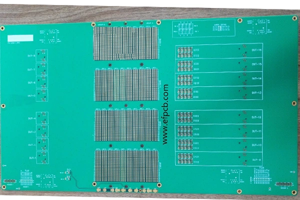
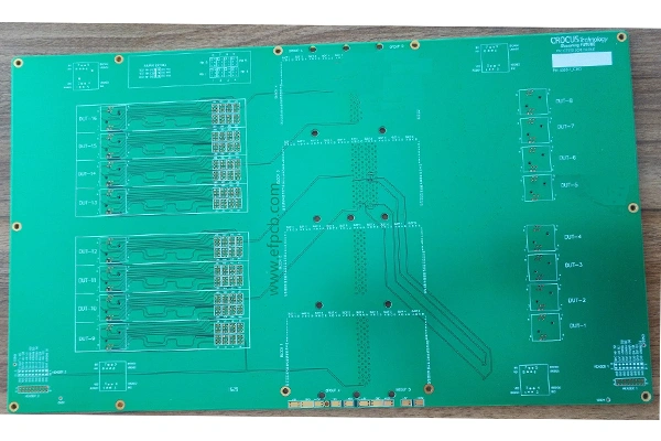
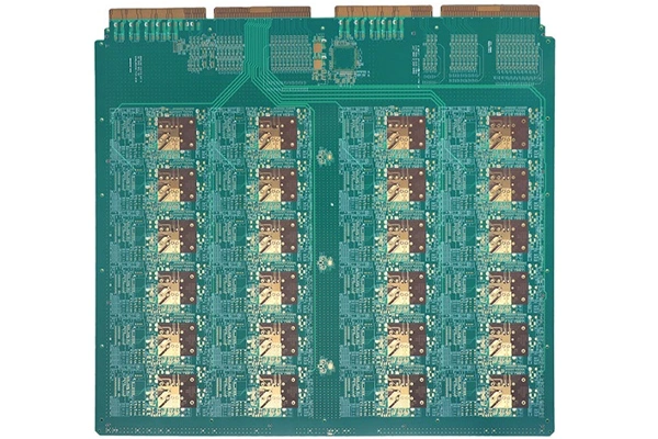
Part No.: E2615060179A
Layer count:26 layer
Material: FR4, 3.8mm,0.5 OZ for all layer
Minimum track:2.8 mil
Minimum space: 3 mil
Minimum hole: 0.40mm
Surface finished: Flash gold
Panel size: 798*278mm/1up
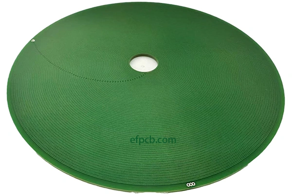
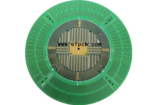
Backplane PCB are key for high-performance systems because they ensure robust connectivity and signal integrity for complex electronic applications. These circuit boards are commonly used in telecom, data center, aerospace and industrial automation as a means to connect several daughter boards. As a professional backplane PCB manufacturer, we are in the position to provide the high quality large size PCB that can be used for high speed signals and large amount of data transmission.
It is special type of circuit board that connects various printed circuit boards and acts these boards to communicate with each other. They tend to be relatively large and are generally multilayered, with a high number of connectors and the ability to handle fast data rates. Backplane PCBs are vital in equipment where signal routing and density matter.
Fabrication is a very technical layer requiring accuracy and high level of machinery and knowledge to achieve maximum performance.
Selection of material
The production starts with choosing the right high-performance materials. Materials are usually required to have good thermal stability and low dielectric loss to carry high-speed signals. As an experienced backplane PCB manufacturer, we provide high-quality materials, like high TG FR4, polyimide, and Rogers laminates, to serve the complexity of your applications.
Layer Stack-Up Design
Backplane PCBs are done as multilayer boards, some more than 20 layers. The stack up is intentionally (layer) designed to optimize signal integrity, power delivery, and impedance control. Sophisticated CAD software is applied for exact registration and crosstalk between layers minimized.
Drilling and Plating
Thousands of vias including through-hole, blind, and buried vias are often necessary to electrically connect between layers. A high precision drilling machine is used to drill these vias, followed by copper plating to guarantee good conductivity.
Signal Routing and Impedance Control
Signal routing is one of the most important factor in backplane PCB production. Controlled impedance is also necessary for high-speed data transmission. As a professional backplane PCB manufacturer, we employ the latest simulation software and design methodologies to limit signal degradation and produce consistent performance.
Assembly and Testing
Backplane PCBs tend to be large, and the assembly also requires close attention to handling. After the boards are packed, they are tested rigorously, including signal integrity test, impedance test, thermal stress test, etc. for compliances of industry standards and customer specifications.
As the top backplane PCB manufacturer, we specialize in manufacturing complicated, large-size PCBs for high-performance uses. With our sophisticated facilities and qualified engineering team, we are capable of providing customized solutions to fulfill diverse needs.
We are experts at high layer count backplane PCB solutions with tight impedance control, excellent signal integrity and dependable performance. Our dedication to quality means that for each and every product we ship, we are confident it meets or exceeds industry standards.
Backplane PCBs serve as the backbone for high-performance systems allowing multiple parts to interact and communicate efficiently. Working with a professional backplane PCB manufacturer is crucial to guarantee your designs turn out reliable and functioning. You can rely on us for quality backplane PCB or backplane PCB assembly and contribute towards seeing your products come alive from design to manufacture to supply.