-
Mail Us Todaysales@efpcb.com
-
Company LocationShenzhen, Guangdong, China
-
+86-755-23724206Call us for more details
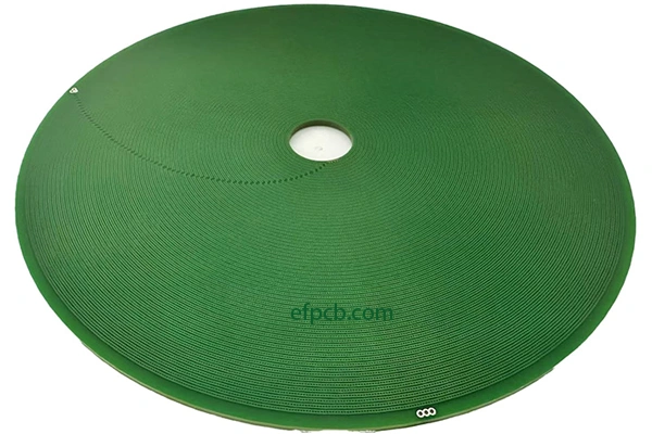
Model: E3614040150A
Layers: 36
Thickness: FR4 High TG, 4.2mm, 1 OZ for all layer
Hole Size: 0.30mm
Line : 5mil
Space: 5 mil
Panel size 270*270mm/1up
Surface Treatment: Leadfree HASL
Characteristics: FR4 high TG, planar winding PCB, high multilayer
Requirement of high multilayer PCB (Printed Circuit Boards) has been increased dramatically with the development of electronics, communications, and computing in recent years. High multilayer count PCBs are integral to many of today's devices, allowing for the complex implementation of multiple devices in a single circuit board. But producing high multilayer PCBs is an intricate and highly specialized process and calls for state of art technology, engineering and quality control. In this article we will discuss the step-by-step process to manufacture high multilayer PCB and focus on the particular concerns, difficulties and best practices.
A CB refers to some layers of conductor patterns (usually copper layers) in more than two, the layers of each layer are separated by insulating materials (resin material or other materials). These are usually at least ten-layer boards, some in high-end designs may be more than fifty layers. High-layer/multi-layer PCBs are used in aerospace, automotive, medical, telecommunications and consumer electronics industry where compactness, reliability and performance are key factors, respectively.
An important feature of a high layer count PCB is that it can host more complex circuitry, as well as keeping a compact form factor. These are boards that offer greater routing density, better signal quality and lower EMI impact, and hence are highly valuable in the world of high-speed and high-frequency design. Critical steps in the fabrication of High Multilayer PCBs
High Multilayer PCB Manufacturing is a Complex Process Making one high multilayered printed circuit board is a complex and several step process that demands precision and skill. The manufacturing process is also illustrated in detail, as per the following:
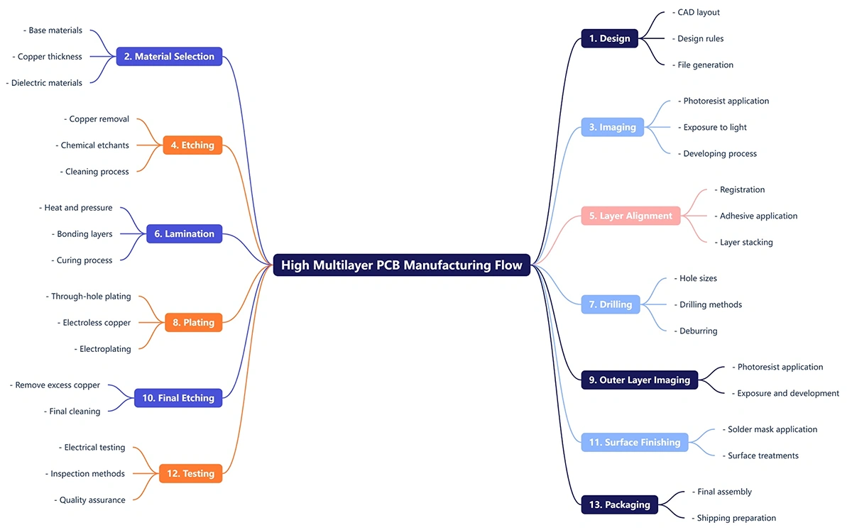
1. Designing the PCB Layout
High multilayer PCB Fabrication The first step to creating high multilayer PCB is a good design. The PCB layout is designed with the help of computer-aided design (CAD) systems – for example ADVANCE. This will comprise pin-out location of components, route of signal tracks, location of power and ground planes and so on.
Important aspects to consider in the design:
Design validation with an imitation of the inducer is carried out to avoid possible problems before manufacturing.
2. Material Selection
The selection of those materials, however, is an important factor in the performance and reliability of high multilayer PCBs. Some common materials used are:
Substrate: FR4 is used in most cases but for high frequency applications, material like Rogers, polyimide, or Teflon may be recommended.
Copper Foil: High-quality coppers exhibiting high conductivity and FPCs are applied for the product in terms of conductive properties.
Prepreg & Core - The insulating materials that bond the layers of a PCB together & add strength.
The materials must be selected to fit the particular needs of the application--for example, high thermal resistance is required, low dielectric constants are demanded, or high frequency performance is needed.
3. Inner Layer Preparation
The fabrication is initiated with the inner layers. These are done as follows:
Photoresist Application The copper-clad laminate is applied with photosensitive film.
Image transfer: PCB design is transferred onto the photoresist layer by exposing to UV light. Light-affected areas become hard, while the unexposed areas are soft.
Etching: The undesired copper is chemically etched, move the copper areas behind the mask.
Inspection: Inspection of the etched layers is carried out with the help of automatic optical inspection (AOI) systems.
4. Alignment and lamination of the layers
Regions of the core are then prepared and stacked together with prepreg and core materials in a desired order once the internal layers are ready. Accuracy matters at this point in order to have all layers nicely together.
The stack is then laminated such that:
Heat and Pressure: The stack is then pressed together in a press while at high temperature, causing the prepreg to melt and form a bond between the layers.
Cure the lamination stack is cured to cure the bonds and generate a solid PCB.
5. Drilling
Vias are then drilled using holes drilled into the PCB to join all layers. The holes are located and sized using a high precision CNC drilling machine.
The vias in high multilayer PCBs come in the following types:
6. Plating and Copper Deposition
After the holes are isplled, the holes are plated with copper to provide electrical connection between the layers. This involves:
7. Imaging and Etching the Outer Layer
It is similar to the inner layers: 3.2 Outer Layers The outer layers are processed in the same way.
Application of Photoresist: A photosensitive film is coated to an exterior side.
Image Transplant: A circuit pattern is transplanted by UV light exposure.
Etching: Any copper that is not covered by the resist is etched away, leaving a patterned circuit of conductive copper.
8. Solder Mask Application
A layer of solder mask is used to encapsulate the PCB and its copper traces to prevent solder bridges during assembly. The process involves:
9. Surface Finish
The exposed copper surface is coated with a surface finish to protect the copper and provide acceptability for solder. Some of the popular surface finishes for high layer count PCB include:
10. Testing and Quality Control
Testing is a very important process to guarantee the functionality and the reliability of the high multilayer PCB. Sequence tests generally are performed using:
Difficulties in the Fabrication of High Multilayer PCB
There are numerous problems that need be resolved when manufacturers produce high multilayer PCBs’ products, such as:
High precision requirement: It becomes hard to maintain the alignment and higher precision as the layers grow.
Material Selection: It can be difficult to locate materials that meet the desired performance, but are economical.
Thermal Issues: High multilayer count PCBs produce a lot of heat that needs to be dissipated.
Cost: Due to the sophistication and requirement for sophisticated equipment, high multilayer PCBs are more costly to manufacture.
Time to Summary of cost cost High Multi-layer PCB manufacturing Tips In order to make high multilayer PCBs, producers must use the following best practices:
Work with EMPOWERED Designers: Partner with experienced PCB designers to prepare the layout to be manufacturable.
Invest in the Latest Equipment: Utilize cutting-edge equipment for drilling, plating, and testing.
Run Strict Quality Control: Check and test at all stages of manufacturing. Select Dependable Suppliers: Find trustworthy suppliers for good quality materials.
Conclusion
High multilayer PCB production is a complicated and highly specialized process that demands precision, knowledge, and high-end technology. From layout, material selection, alignment of layers and thorough testing, each step is critical to the overall quality and reliability of the end product. Manufacturers are able to manufacture high multilayer PCBs to the strict standards required by today’s electronic devices by adhering to best practices and addressing challenges. With the development of technology, the requirement to use the high multilayer PCBs will become more and more significant and it is becoming an indispensable part of electronic future.