-
Mail Us Todaysales@efpcb.com
-
Company LocationShenzhen, Guangdong, China
-
+86-755-23724206Call us for more details
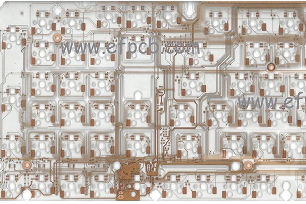
Layer count: 2 layer
Material: Transparent material, 1.6 mm, 1 OZ for all layer
Minimum trace: 300 um
Minimum space(gap): 300 um
Minimum hole: 0.40mm
Surface finished: OSP
Panel size: 230*78mm/120up
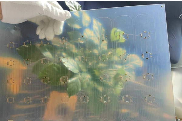
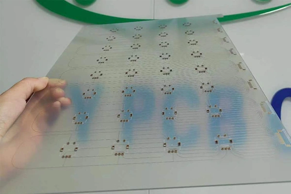
Characteristics: Transparent
The world of printed circuit boards (PCBs) is moving to significant and change, and at center stage of that change is the Transparent PCB. Welcome 2025, and the Transparent PCB demand is fueled across sectors from the consumer electronics to medical and automotive systems and many more. In this article, the technology, advantages and manufacturing methods of Transparent PCBs gets elaborate to make an extremely smart and useful guide for electronics engineers, designers and tech geeks.
A transparent PCB is a type of circuit board which is both conductive and transparent that make it perfect for embedding into displays, touch screens, and more onto smart surfaces. While traditional opaque PCBs use inorganic materials like glass covered with silver or copper films, Transparent PCBs incorporate state of the art materials such as a transparent conductive oxides (TCO), conductive polymers or ultrathin metal meshes that have electrical function together with light-passing capability.
The Transparent PCB will experience an increase in 2025 due to the want for thin and comely wearables techs, augmented realities (AR) glasses along with foldable smartphones Amber waves of gen. Companies that use Transparent PCBs are able to differentiate themselves by delivering products that look better and work better.
A first-class feature of the Transparent PCBs is their capability to integrate well with display technologies. In both OLED and micro-LED displays, Transparent PCBs allow for incredibly thin, flexible designs that still maintain drive and signal performance. Moreover, their transparency allows them to serve as heads-up display (HUD) systems in car dashboards and aviation.
Durable another big advantage: Manufacturing. In 2025, transparent PCBs based on substrates that have been reinforced with high-strength composition like tempered glass or polyimide film to resist bending, heat and environmental stress.
Such that, these characterize the essential superior processor of future foldable and solar panels in outdoors electronic sign ages.
Exposing Transparent PCBs: Modern Methods of Making
Creating Transparent PCBs is a challenging technique that needs the precision engineering and extensive fabrication processes. The typical modes of operation are as follows:
The production of Transparent PCBs is done with a series of processes to ensure optical clarity and electrical conductivity. Here is a detailed process in line with the practices of today industry? Material Selection and Substrate Preparation
Core Materials:
Polyimide films, tempered glass or flexible polymer sheets (PET/PEN including) (transparent substrates)
Conductive layers: sputtered indium tin oxide (ITO), graphene or a thin metal mesh (copper/silver).
Pre-treatment: Plasma cleaning of substrates for adhesion improvements in conductive coatings.
Circuit Patterning
Photolithography:
Defined on a conductive-coated substrate, the photoresist layer
Photoresist transfer of circuit pattern followed by chemical etching (plasma) to remove all the unexposed that remain.
Laser Direct Imprinting (LDI): High-accuracy lases etch circuits for small-pitch circuitry (<10 µm).
Etch and Forming of Conductive Layer
Anisole Etching: Usually acidic solution (e.g., ferric chloride that remove excess conductive material, only remaining traces are desired).
Plasma etch: Enhances precision with minimal undercutting for high-density interconnects.
Alternative Methods
Fabrication of conductive transparent polymers (e.g., inkjet printing of poly).
Mass production using Nanoimprint Lithography
Screen to Multi-Layer PCB (How layers are stacked & lamination in PCBs)
Adherence: Transparent adhesive layers (i.e. optical clear-resin) interpose between more circuit layers with <5µm offset.
Vacuum Lamination: Cures transparency from air bubbles.
Drilling & Via Formation
Laser Drilling: Femtosecond lasers make dense micro-vias (<50µm diameter) with limited heat-affected zones.
Conductive via filling: UV-curable conductive resins provide inter-layers connection without opaqueness.
Surface Finishing & Functionalization
Protective Coatings:
Atomic layer deposition of alumina for water resistant.
Anti-Reflective coatings which transmit light (>90%).
Flexible PCB Enhancement: Blueprints are folded with elastomeric substrates for bendable forms.
Quality Control & Testing
Optical Inspection – Automated systems inspect micro-cracks or conductive defects.
Electrical Testing:
4-point probe measurements s/r sheet resistance (<100 Ω/sq).
Terahertz imaging confirms signal integrity for high-frequency performance.
Yield Manipulation: AI and process control reduce defects for massively larger area panels.
Sustainability: Recyclable transparent polymers instead of your regular stuff
This approach allows Transparent PCBs for applications like AR displays, smart windows and biomedical sensors. Material-specific or equipment recommendations should be the topic of discussion with specialist producers. The 2025 manufacturers are jumping on-board with AI-driven quality inspection tools to produce Transparent PCBs defect-free and ensuring that signaling loss is minimized between for most efficiency.
Due to the wideness of applications in which Transparent PCBs are used;
Consumer Electronics: Bezel-less displays and touch-sensitive surfaces for phablets or smartphones, tablets and smartwatches.
Medical: transparent circuits for instruments like screens of diagnostic equipment or wearable health monitors.
Automotive & Aerospace: Augmented reality windshields; displays in cockpit
Architecture/Smart Glass: Economically smart windows equipped with the WiFi sensors, rest the bond layer and/or information embedded throughout into a transparent PCB.
2025 onward, we will see further improvements with transparent PCBs:
Bio Self-healing Circuits: materials that can naturally heal minor damages over time, keeping the survival of Transparent PCBs.
Polymer substrates: biodegradable transparent polymers that are reducing e-waste waste
Quantum Dot Integration: Ensures accurate display color with improved energy efficiency in TPCB-based screen.
Instead of a far-fetched fiction the Transparent PCB is defined as we are crafting tomorrow's electronics. The Transparent PCBs are going to take over all tech in the year 2025 and above, with sky-high design excellence and durability… If you be an engineer, product designer or tech enthusiast in 2018 and turning ahead — you need to get smarter with transparent and using PCBs. One thing is certain, the pace of innovation only quickens — the future of electronics is clearly going to be translucent.