-
Mail Us Todaysales@efpcb.com
-
Company LocationShenzhen, Guangdong, China
-
+86-755-23724206Call us for more details
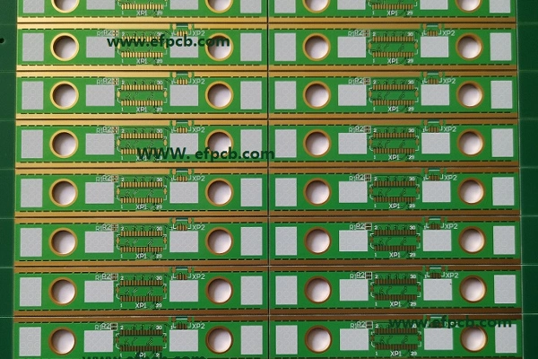
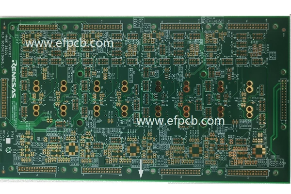
Layer count: 6 layer
Material: FR4, 2.0mm, 1 OZ for all layer
Minimum track: 6 mil
Minimum space: 6 mil
Minimum hole: 0.25mm
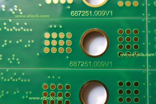
Surface finished: ENIG+Hard Gold (Au>30U")
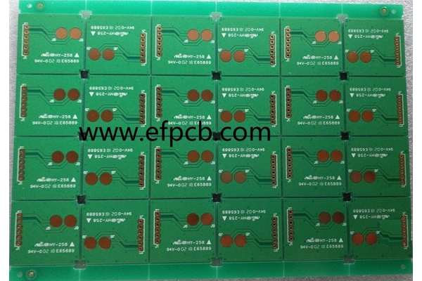
Panel size: 268*198mm/20up
Hard Gold Circuit Boards are also the foundation of high-reliability electronics and are used in applications where superior performance and toughness are required in the most extreme environments. To any realistic PCB manufacturer, understanding the complexity of hard gold plating is pivotal. In this piece, we will describe the manufacturing process of these special boards and some of the crucial attributes that make our product superior.
A hard gold PCB is made up of a thick gold plating which is normally present on contact areas, edge connectors, and keypads. In contrast to soft gold, hard gold is an alloy, generally with cobalt or nickel, making it much more wear-resistant and harder. This is most important in parts which are removed and inserted a great many times, like memory sticks or expansion cards. The level of hard gold plating can range where it may be 3 to 50 micro inches depending on the level of wear resistance and thermal and electrical conductivity required. The main benefit of Hard Gold Circuit Board is in its high wear and corrosion resistance. This is why it is perfectly suited for military, aerospace, medical and advanced industrial usage where reliability is critical. A good PCB manufacturer knows that this gold layer quality will influence the working life and the EEPROM of the final electronic product.
The process from a PCB manufacturer's perspective
There are many critical stages in the fabrication of a Hard Gold Circuit Board, all of which must be closely monitored and handled with care by the PCB manufacturer.
Copper surface of PCB needs to be perfectly clean before gold plate. It includes several cleaning, degreasing, etching. Any contaminants or oxides on the copper surface will weaken the bond, as well as the subsequent layers plating. Any residual contaminants or oxides on the copper will negatively affect the adhesion and integrity of the subsequent plating layers. This step is very important in order to get even and good gold depositing.
An electroless or electrolytic nickel deposit is applied after surface treatment. This nickel acts as a barrier layer that stops copper from diffusing into the gold, and also adds more hardness and wear resistance to the surface of the contact. The thickness and quality of this layer of nickel is critical, and is typically between 100 and 200 micro inches. An experienced PCB maker ensures the uniformity of this layer so as not to introduce particles of “black pad”, which results in bad solderability or pad joint cracking.
This is the unique process that makes Hard Gold Circuit Board. The gold is normally deposited via an electrolytic process, which uses electric current to deposit solid gold ions over the nickel-plated surface. The gold bath solution contains additives like cobalt or nickel which co-deposit with gold at a certain co-deposit rate. Proper control of current density, plating time and solution chemistry is required to attain/class the desired gold thickness and composition of the alloy. Sophisticated plating technologies and trained personnel are required in this stage to obtain full thickness and even quality over all plated features.
The gold plated boards are rinsed after the plating process to remove any chemical residue from the plate. Then, there is drying, and an all-round inspection. This inspection comprises visual examination for defects, thickness determination with X-ray instrument, adhesion tests. A good quality-conscious PCB manufacturer will even carry out electrical testing to confirm that the circuits have not been damaged and the gold plated contacts function correctly. In short, production of a Hard Gold Circuit Board is nothing less than a work of art. Topxyzxyz1 When your hard gold or ENIG PCB vendor is best in class, the excellence of their strict vibrant process control from prior to starting surface pre-treatment to final testing will be a world of differences, not only in raw for your high capability PCB (PCBA) but the best ultimate dependability and performance to execute in your hardest electronic applications.
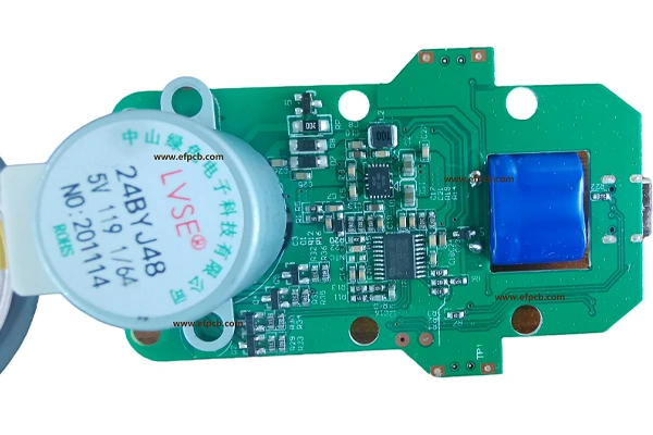
Hard gold PCB application for Automobile.