-
Mail Us Todaysales@efpcb.com
-
Company LocationShenzhen, Guangdong, China
-
+86-755-23724206Call us for more details
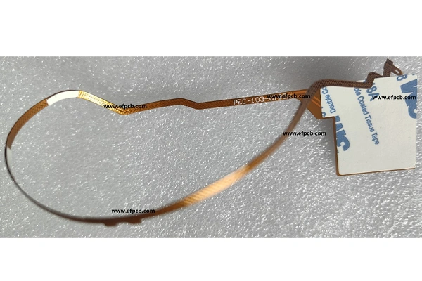
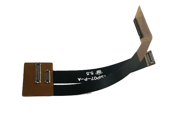
Part No.: E0215060979P
Layer count: 2 layer flex PCB
Material: Polymide, 0.15mm,0.5 OZ for all layer
Minimum tack: 8 mil
Minimum space(gap): 5 mil
Minimum hole: 0.25mm
Surface finished: immersion gold
Panel size: 298*28mm/1up
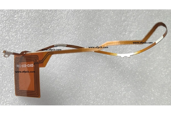
In the fast-paced world of intelligent contactless smart gadgets, NFC (Near Field Communication) flex PCBs have become critical components for smart and secure wireless data transmission. As more and more consumers pursue thinner, more flexible and highly dependable circuit solutions, the expertise of an NFC flex PCB maker would prevails. This article analyzes the production process and the main product features of a professional NFC flex PCB manufacturer in the current market.
What is an NFC flex PCB manufacturer? Having 30+ years of experience Flex PCB, Rigid Flex PCB, Rigid PCB production, High Quality PCB is able to produce the best quality NFC flex PCB manufacturer with high technology and most competitive prices with free. The sign of a good NFC flex PCB manufacturer with excellent signal integrity or they can provide circuits with ultrathin thickness and high durability. The flexible substrate (commonly polyimide) enables the PCB to bend and twist to multiple degrees and angles, making it suitable for small and rounded device enclosures. Sophisticated Manufacturers employ fine line etching and precision laser cutting to form sophisticated patterns for the antenna, enhancing the transmission of signals while reducing the losses. In addition, trustworthy producers make sure their products comply with environmental and electrical requirements such as RoHS and high-frequency standards.
So the journey starts with selection of materials. A leading NFC Flex PCB manufacturer adopts high-quality polyimide films and high-purity copper foils to provide excellent flexibility and conductivity. The substrate is cleaned to remove any contaminants that may interfere with circuit performance. Subsequently, the antenna pattern is printed on the copper clad film using high-tech imaging methods like the LDI process. This procedure is important because the shape of the antenna has a big impact on the range and reliability of the NFC signal. The copper that is not covered is then etched off, and the precise antenna pattern remains. Then lamination is followed if any layers added for shielding or capping. The NFC flex PCB manufacturer controls the process of lamination to the extent that the flexibility of the board can be maintained and its mechanical strength be increased. If need be, laser drilling is used to create microvias and component pads, allowing exact alignment and connection for the NFC chip. Surface finishing is another essential process. The NFC flex PCB producer uses finishes such as ENIG (Electroless Nickel Immersion Gold) to enhance solderability and protect copper from oxidation. The board is then put through extensive electrical test and AOI to assure the performance is perfect. Ultimately, the NFC flex PCB maker wraps the done circuits in protective materials, for use in smart devices. Through the use of innovative materials, precision engineering and rigorous quality assurance a world class NFC flex PCB manufacturer can provide products that allow for secure, efficient and dependable NFC technology for the future of electronic applications.