Flexible circuits appear very straightforward on the surface, but the path of production is an airpressurised chain of events where every link influences bend life, electrical conductivity, and assembly output. This introduction will guide you through a representative flow of a leading-edge
flex PCB manufacturer, discussing what goes on in the real world and on the production floor and how those realities impact what you get and what you pay.
Design Intake and Process Planning for Flexible PCB
Before being cut, the work is also converted into a build procedure that manufacturing can use as a baseline. A professional flexible PCB manufacturer that understands the products and the application area will check the Gerber files, the stackup, the impedance, the bending areas, and any other component specific limitation that they can consider as process limitations. Important good practice checks include:
• Minimum trace and space to chosen copper weight.
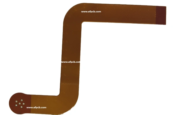
• Bend radius recommendations and distribution of copper uniform to minimize cracking risk.
• Coverlay openings, pad support, tear-stop features.
• Drill strategy for vias, microvias requirements.
• Panelization scheme for stable handling through multiple wet processes.
Flexible PCB Material Preparation and Surface Conditioning
Flex circuits typically begin with polyimide-based copper clad laminates. The handling of the materials is important because contamination and moisture can trigger loss of adhesion. In a tightly controlled flexible PCB manufacturer line, materials are baked or conditioned as required, cut to panel size and cleaned to ensure adhesion. Typical preparation is:
• Incoming inspection for thickness, copper type, and surface quality
• Cleaning and micro-etching of copper to prepare for imaging and plating
• Humidity-stabilizing, dimensionally drift-reducing Environmental controls for Product Consistency Imaging, etching, and circuit pattern definition Circuit elements are formed by patterning copper and then etching away the excess. A detailed sensitive quality-conscious flexible PCB manufacturer adjust exposure energy, developer chemistry and etch rate in order to safeguard the fine line, and to maintain uniform line width across the panel. Basic stages:
• Photoresist lamination (for uniform coverage)
• Laser plotting or direct imaging for registration precision
• Developing to expose copper to be removed
• Etching and resist removal to form finished traces
• Automated optical inspection:This is to detect opens, shorts, and line width deviations as early as possible Drilling, via fabrication, and copper plating Interlayer connections and component holes must be clean and crisp. Multilayer flex or rigid-flex, this stage has a major impact on reliability.
• A professional flexible PCB manufacturer chooses mechanical drilling, laser drilling or a combination of both, and then metallizes the holes. Drilling with controlled parameters not to produce burring and smearing
• Desmear and hole wall conditioning to provide good copper adhesion
• Electroless copper seeding, followed by electrolytic copper deposition
• Thickness measurement to satisfy the required current density and reliability
Lamination, Coverlay and Layer Bonding
Many flex builds involve bonding multiple layers, or adding coverlay for insulation or adding stiffeners. This is where pressure, temperature, and time under heat separate a solid piece from a cross-hatch panic. A Professional flexible PCB manufacturer will have proven lamination profiles and high cleanliness levels. Typical procedures:
• Layup registration and alignment
• Curing of thermal compatible adhesive systems in a laminating process.
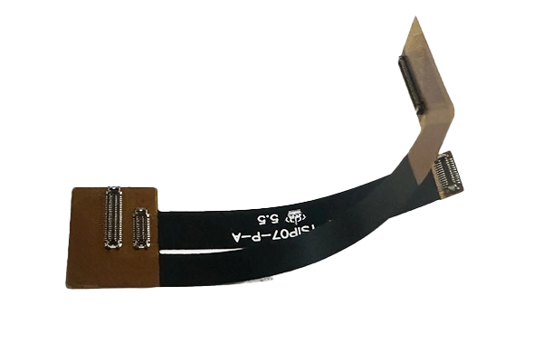
• Coverlay with windows for pads and test points - Stiffener attachment in connector and component areas
Surface Finishing, Final Machining, and Electrical Testing
Once the circuits are formed and protected, the surface needs to be able to be soldered and resist corrosion. This flexible PCB manufacturer for production is supply the surface treatments like ENIG, immersion silver, OSP according to the assembly process, storage cycle and finished with final profiling. Basic necessities for final stage:
• Deposition of surface finish with bath control and thickness inspection
• Legend Marking where applicable; clear of bend areas
• To final outline accuracy by routing, laser cutting or punch cutting
• To verify continuity and isolation - 100% electrical tested
• Visual inspection and dimensional checks, packaging to prevent wrinkles etc.
What Flexible PCB Process Control Means in Terms of Actual Reliability
Flex circuits fail most at the interfaces - plated holes, bend transitions and stressed pads. A proven flexible PCB manufacturer creates reliability within the production process with in-process inspection, micro sectioning and traceability of raw material lots to finished panel. The practical conclusion is this: When everything is controlled and documented, predictable soldering is the result which leads to stable impedance and longer bend life. That is the standard that customers should expect from a trusted multilayer PCB manufacturer.
Medical Device Sensor Application