-
Mail Us Todaysales@efpcb.com
-
Company LocationShenzhen, Guangdong, China
-
+86-755-23724206Call us for more details
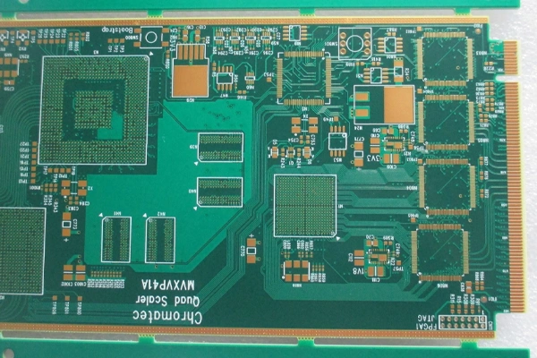
Part No.: E1215060189A
Layer count: 12 layer
Material: FR4, 1.6mm, 1 OZ for all layer
Minimum track: 5 mil
Minimum space: 5 mil
Minimum hole: 0.20mm
Surface finished: ENIG + Hard gold (Au>3um)
Panel size: 228*108mm/1up
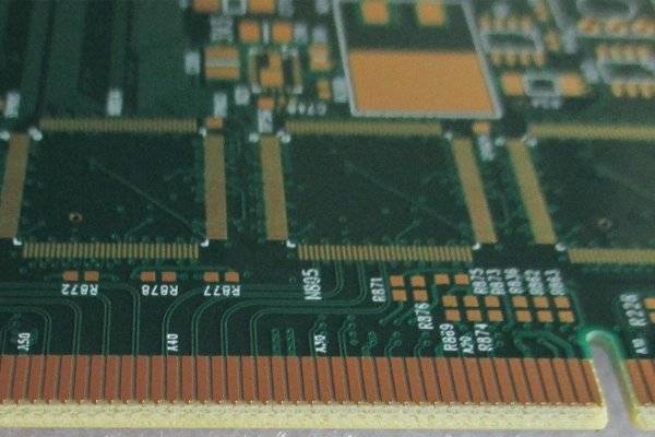
Edge connector PCBs (popularly called gold finger PCBs) are vital parts of today’s electronics industry ensuring solid connections between PCB and another entity. Their one-of-a-kind shape-which includes gold-plated contacts on the edge-requires a careful manufacturing process to attain best results. As a top gold finger PCB manufacturer in the industry, we provide high quality edge connector PCB to meet your different demands.
The design of an edge connector PCB starts with choosing suitable base materials. Usually, FR-4 is the laminate utilized because of good electrical and physical attributes. But you may come across with other materials for high frequency application, such as high-TG FR-4 or even ceramic-filled type. The PCB thickness, number of layers, and copper weight are application specific. The most unique aspect of an edge connector PCB is its gold fingers. Rather, they are complex contact pads that flow out from the edge of the board. The decision for gold plating is important. Hard gold is normally a term for an alloy of gold and cobalt or nickel and has a great resistance to wear and conductivity so it can be used for multiple insertion and removing. The gold thickness of the plating is also very important, which is generally from 3 to 50 micro inches based on the ended mating cycles and environmental condition. Ours as an edge connector PCB manufacturer assures maximum accuracy in above specifications.
There are many complex processes in production of gold finger PCB, need each to be controlled strictly by quality.
The process begins with the base PCB manufacturing, which consists of drilling, etching and multi-layer lamination. When the substrate printed circuit board has formed, the gold finger part is plated. It includes a nickel barrier deposit for the copper, followed by the gold. Nickel also stops the copper migration under the gold which can impact the electrical performance over time. After nickel plating, then hard gold is electroplated on the contact pads. This electrolytic processing gives a consistent and hard gold layer. As a professional gold finger PCB manufacturer, we adopt modern plating technique to get high uniformity and adhesion.
The edges of an edge connector PCB are usually beveled after gold plating the edge connector PCB. This chamfering process, usually performed at an angle of 45 degrees, allows for smoother entry into the other connector and minimizes the friction between PCB and connector. It is important to know how to bevel precisely without ruining the gold fingers! The last phase involves extensive quality control. This entails a visual examination to detect flaws, measurement of the thickness of the gold plating by X-ray fluorescence (XRF), and electrical testing for continuity and dielectric integrity. Our responsibility as an edge connector PCB manufacturer raises to a level of the whole testing procedures, in which every edge connector PCB that are us shipment reaching are tested at the highest standards in the industry.
The selection of a suitable gold finger PCB manufacturer is crucial in ensuring your electronic products perform well. We're unique because of our:
When you work with us, you can rest assured that you will get high-quality, dependable edge connector PCBs which enable your electronic devices to work at their best.