-
Mail Us Todaysales@efpcb.com
-
Company LocationShenzhen, Guangdong, China
-
+86-755-23724206Call us for more details
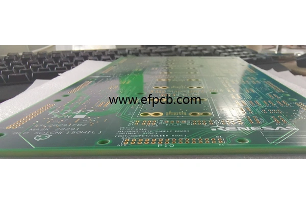
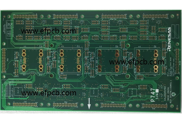
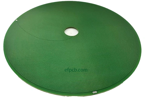
Layer count: 8 layer
Material: FR4, 2.0mm, 1 OZ for all layer
Minimum tack: 5 mil
Minimum space: 5 mil
Minimum hole: 0.20mm
Surface finished: full board Hard Gold (Au>30U")
Panel size: 368*108mm/1up
Hard gold PCBs have many applications in the fortunes of high operating conditions, mainly because of high toughness, good conduct, and best wear-resistance. These PCBs are especially found in semiconductor test boards, high frequency devices, or connectors with recurrent mechanical contact. Hard gold, also referred to as electroplated gold, is deposited on certain portion of the PCB to offer a strong surface finish that is able to endure severe environment and continuous use.
Producing a hard gold PCB is a complex process that demands accuracy, focus and compliance with rigorous quality standards. In this article, we will share with you the entire hard gold PCB process to manufacture it and its unique features to achieve the maximum result.
Hard gold is a type of surface finish that is applied to PCBs, a via cohesive process. Unlike softer finishes such as immersion gold, hard gold is a thick layer of gold alloy (gold with cobalt or nickel) that has exceptional hardness. It is found also on high-reliability applications such as semiconductor test boards, edge connectors and keypads.
The depth of hard gold plating is usually from 30 to 50 microinches (0.76 to 1.27 microns) according to the type of work. Corrosion-resistant, wear-resistant and non-tarnishing properties make hard gold a good choice for uses that involve frequent mechanical interaction and extreme environmental conditions.
Substrate Materials of Hard Gold PCB
The selection of the substrate material is crucial for the performance of the hard gold PCB. For the majority of applications, FR4 is generally used as the base material, except for use on boards intended for semiconductor testing or RF circuits. It is essential that the substrate be a good base for electroplating and can hold up under the rigors of use.
Design for Hard Gold PCB
When you design a board that is going to be plated with hard gold, you have to take that into account when designing the outlines where you want the finish to be applied. Hard gold is most commonly utilized for contact pads, edge connectors, and other surfaces that undergo frequent rubbing or has a low contact resistance requirement.
Some hard gold PCB basic design considerations are:
Selective plating: In order to mitigate the costs and to be efficient in utilizing material, the area for hard gold plating should be defined accurately by the manufacturer.
Trace Width and Spacing: Adequate spacing of gold plated fingers avoids shorting and provides consistent electrical performance.
Thickness control: The thickness of the gold plating must satisfy requirements on the endurance and conductivity of the application.
Pre-Production Procedures
The process of making starts with the PCB design. The manufacturers employ sophisticated CAD tools to design the layout of the board with hard gold plating areas clearly identifiable. Photo tools are generated for each layer of the PCB after the design is complete.
Copper Plating
Copper plating is the first step in the physical manufacturing process. The conductive traces are formed by depositing a thin layer of copper on the PCB’s substrate. This procedure lays the groundwork for a subsequent hard gold plating.
Copper plating is generally done by electroplating – the PCB is immersed in a copper sulfate bath, an electric current is passed and copper is deposited on the exposed portions. It is dated, fast and straightforward, as well as almost unbreakable in the hands of a drunken sailor.
Before Copper Plating and Pattern Etching
Copper plating, apply photoresist and patterning
After copper plating, a photoresist material is coated on the surface of the PCB. This light-activated agent is employed to designate the locations of where the hard gold plating is to be applied. The PCB is exposed to UV light via a photomask, transferring the pattern to the photoresist. After completing the exposure, the photoresist is chemically stripped from the unexposed sections, the copper traces and pads are now exposed to be plated.
Nickel Plating
A layer of nickel is electroplated over the exposed copper areas prior to the hard gold finish. As a barrier layer Nickel prevents the diffusion of copper into the gold and establishes the thickness of the gold plating.
The standard thickness of the nickel layer is about 100-200 μin (2.54 to 5.08 μm).Plating parameters are well-controlled by the manufacturers to obtain the expected plating thickness and conformal.
Hard Gold Plating Process
Hard gold plating is a process in which a gold alloy is deposited on to the nickel plated surfaces. The gold is code posited from bath containing gold salts and a small amount of cobalt or nickel to increase hardness and wear resistance.
The thickness of the hard gold layer is rigorously controlled to satisfy the application requirements. For semiconductor test boards and similar demanding applications, manufacturers generally build a gold layer of 30 to 50 microinches. Application of Solder Mask
After hard gold plating, a solder mask is placed on the PCB to protect the unplated region of the PCB and stop solder bridging throughout assembly. The solder mask is usually screen printed and cured with UV light or heat.
Hard Gold PCB Inspection of Surface Finish
After the solder mask is applied, the PCB is then inspected to verify that it passed the hard gold plating standards. Using technologies including X-ray fluorescence, manufacturers are able to test for gold plate thickness and uniformity.
Quality Assurance and Testing
Durability: The hard gold plate has good wear resistance performance, it can be used on connectors and pads contacts.
High conductivity: Gold provides the best electrical conductivity, which creates an excellent performance in high-speed/high-frequency circuits.
Rust resistance: Hard gold plating can prevent oxidation and environmental damage to the PCB.
Long life: Hard gold PCBs have the production capability to last through 1000 or more mating cycles without meaningful damage.
Applications for Hard gold PCBs find a variety of applications in telecommunication space & SFQ circuits, Nano scale Electromagnetic devices etc. Hard gold PCBs are used in a variety of industries, including telecommunications, aerospace and semiconductors. Semiconductor testing boards, in particular, use this finish due to their need to preserve signals integrity through multiple test cycles. Other typical application is in edge connectors, keypads and high frequency circuits.
The process of making hard gold PCB is a complicated and fine work which demands leading-edge technology and experience. Every process has to be controlled rigorously from the raw material selection and copper plating to nickel and gold plating to make it perform well. For applications such as semiconductor test cards where reliability and accuracy is critical, it is required to work with a professional hard gold PCB manufacturer. These makers possess the expertise and resources to produce quality PCBs that comply with the highest industry standards.