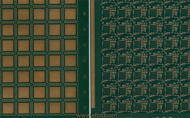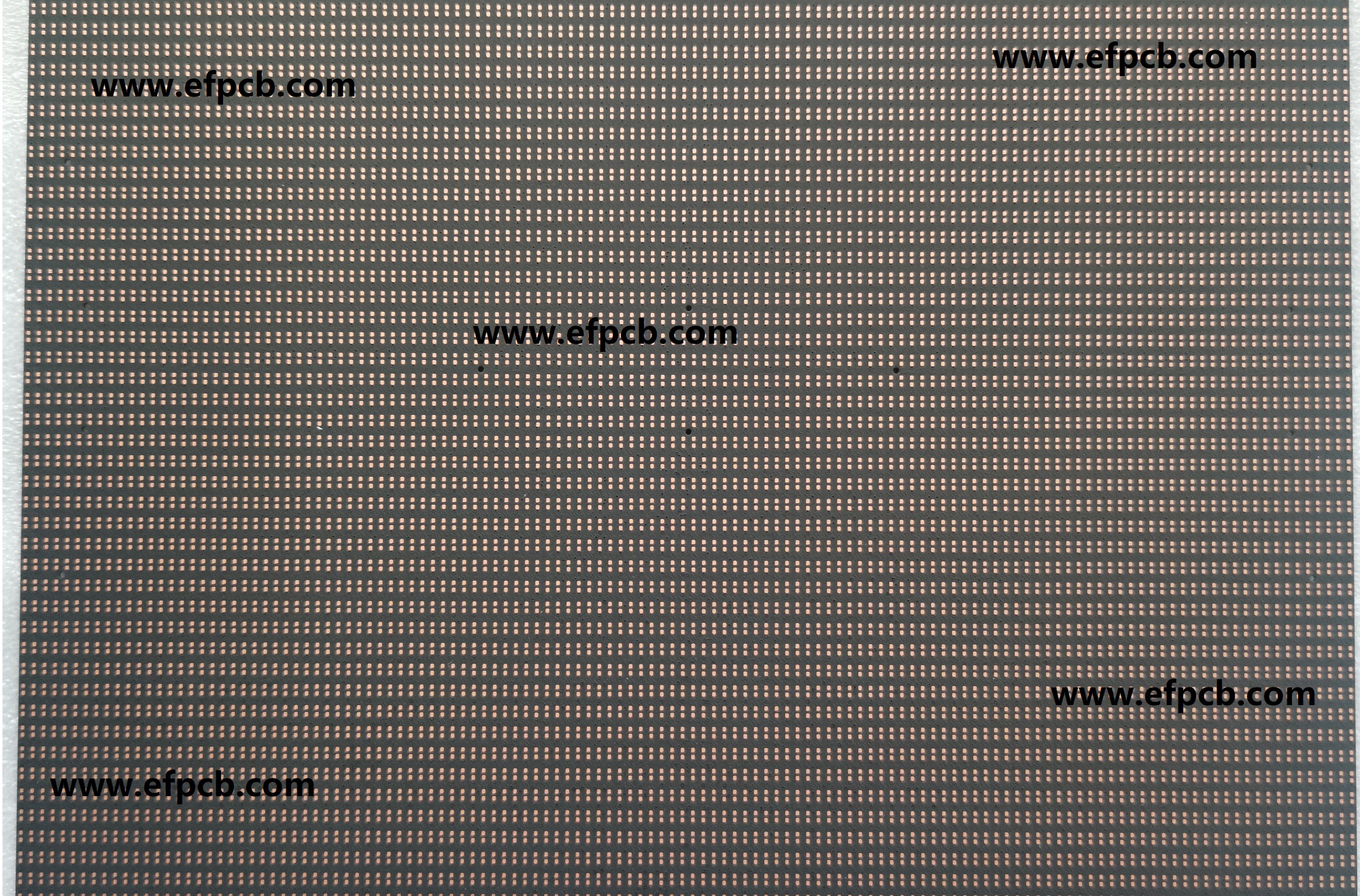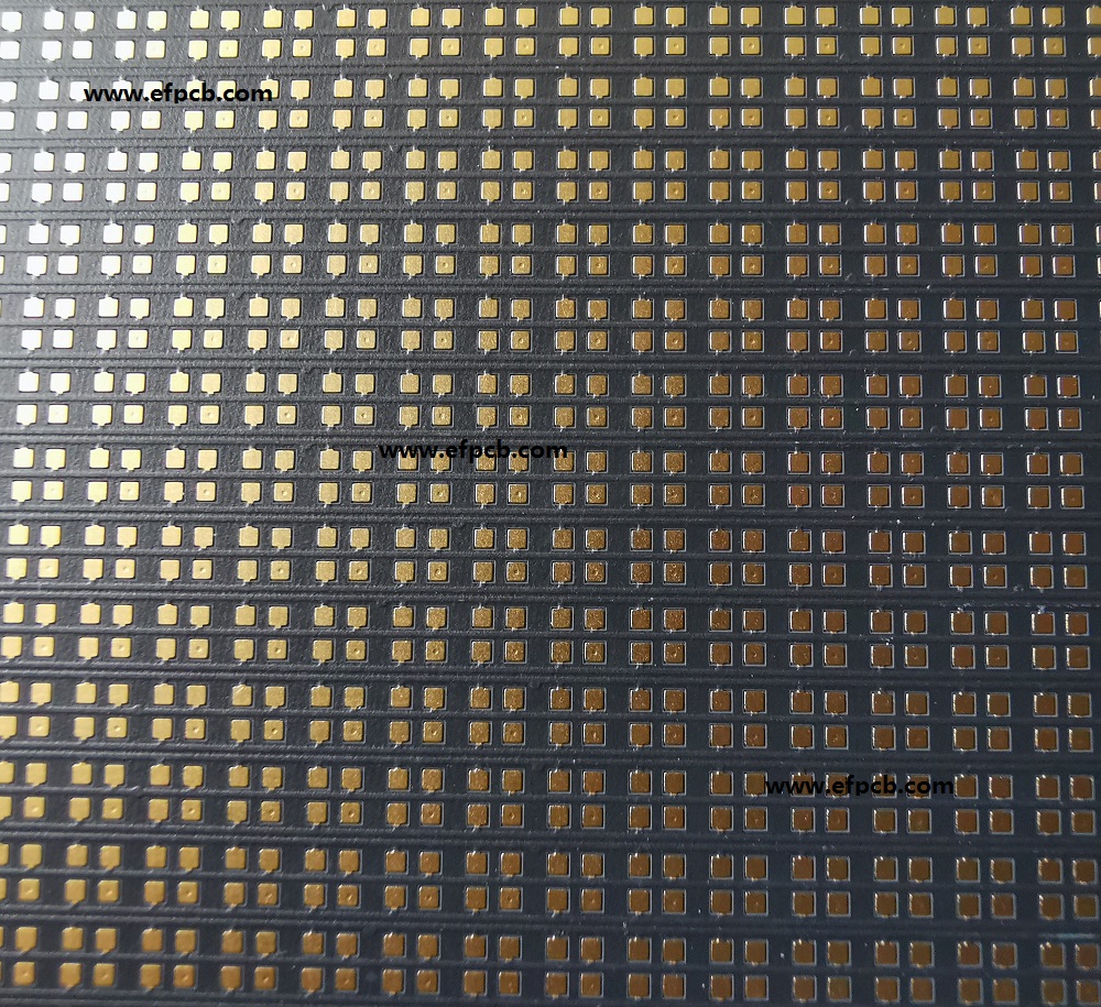
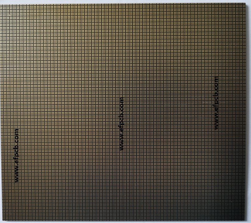
HDI PCB, Micro via PCB, LED display PCB, Via on PAD PCB
Name: VIA ON PAD PCB, HDI PCB, MULTILAYER PCB
Layer count: 6 HDI PCB
Material: FR4 , 1.2mm, TG 180, 0.5 OZ for all layer
Minimum tack: 3.6mil
Minimum space(gap): 3.6mil
Minimum hole: 0.15mm
Surface finished: ENIG
Panel size: 320*268mm/1up
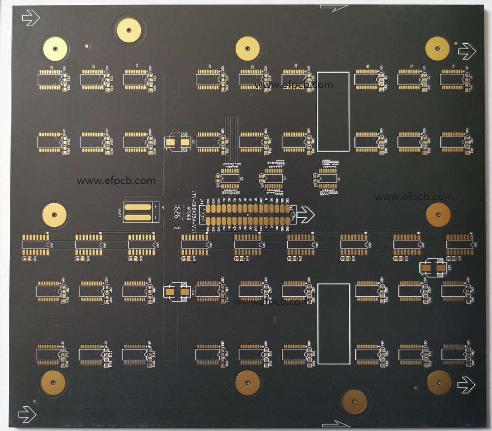
Application: LED Desplay main board
Characteristics: high density interconnect PCB, via on PAD (plug with resin, and plate copper flat), high TG
LED display P1.6 main board,