-
Mail Us Todaysales@efpcb.com
-
Company LocationShenzhen, Guangdong, China
-
+86-755-23724206Call us for more details
Layer count: 4 layer
Material: BT, 0.36 mm, 0.33 OZ for all layer
Minimum trace: 30 um
Minimum space(gap): 30um
Minimum hole: 0.10mm
Surface finished: ENEPIG ( Ni 200U" Pd 2U" Au 2U")
Panel size: 238*72mm/168up
Characteristics: Low CTE, ENEPIG for bonding, BT raw material
The accelerated development of electronic devices has dictated the requirement for smaller, more powerful and reliable printed circuit boards (PCB). Ultra HDI PCB technology is the most advanced in this field offering the potential to provide dimensions and performance the likes of which we have never seen before. This article takes you on a deep dive about the technology with the definition, manufacturing procedure, design rules, applications and development issues in the form of credible data points and industry perspective.
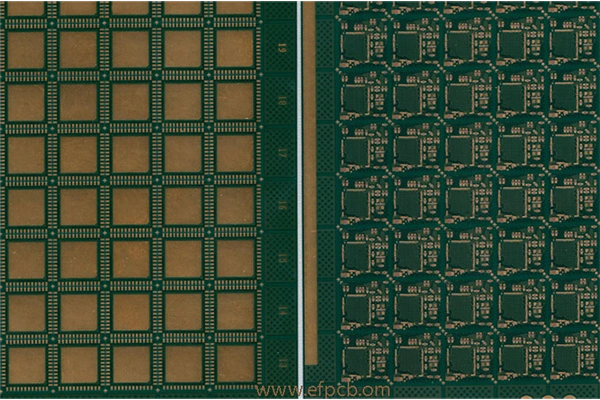
Ultra HDI PCB (Ultra High-Density Interconnect printed circuit board) marks the top layer of PCB miniaturization. By definition, it is having line width and spacing less than 40 micrometers, in addition to microvia setups in diameters under 50 micrometers and mildly thick dielectric layers IPC-2226 defines HDI PCB densities and Ultra-HDI pushes these limits, divisible to support designs supported by multiple interconnects-per-square centimeter than what is enabled by conventional 2-layer buildups.
Ultra HDI PCB is what sets the 4×4 interconnect design feature apart by allowing super intricate routing within such a small footprint. This measured approach is obtained by way of advanced materials, laser-drilled microvias and multiple sequential build-up (MSBU) processes. Hence, the technology plays an indispensable role in today's products particularly for smartphones, wearables, high-frequency RF modules and advanced medical implants.
Creating ultra HDI PCB is an advanced process that relies on different cutting-edge technologies. it starts with substrate selection. The use of low dielectric loss and high temperature resistant materials (modified polyimides) is preferred for increasing signal integrity at high frequencies.
Central to the production of Ultra HDI PCB is laser drilling. In contrast to classic mechanical drilling, the involvement of laser leads to microvia sizes as small as 25 micrometers. These microvias are critical for connecting multiple layers without consuming a lot of space on the board. The process is controlled extremely well, often monitored by an automated optical inspection (AOI) system to verify the quality.
Sequential build-up (SBU) technology is an important part of that other piece of jumbo African fish. This involves laminator and separately patterned dielectric, and copper layers are added one copper at a time, which allows you to have stacked and staggered microvia structures. This way the structure allows for advanced via-in-pad schemes very important in the high density routing of Ultra HDI PCB.
Copper plating and etching processes are also developed for Ultra HDI PCB. To ensure line definition parameters are met, copper thickness is carefully controlled (often less than 15 micrometers). Advanced direct imaging (DI) techniques are used for creating the circuitry as line/space geometries range from 20 /20 micrometers or less.
An Ultra HDI PCB design necessitates a multidisciplinary optimization of electrical, mechanical & thermal constraints. Signal integrity is supreme, especially for data rates that well exceed 25 Gbps in modern devices. Impedance and a serving host of the interconnect issue, via sizing, crosstalk and Electromagnetic Interference (EMI) must be managed by defining the trace geometry and stack-up.
Power integrity is something you can't cut corners with. Because of the dense nature of Ultra HDI PCB all power distribution networks (PDNs) must be designed to guarantee minimum voltage drop and noise. Many of these components are placed in a decapping pattern more or less regularly and aided by embedded capacitance material. The thermal management is a challenge in itself. Localized hotspots can be caused by dense placement of components and thin dielectric layers. Advanced thermal vias, heat spreaders and sometimes microfluidic integrated on-package heat sinks are used to cool the chips effectively.
DFM guidelines for Ultra HDI PCB are very stringent considering that they are a manufacturing aspect. Increased precision and finer features, as well as the use of high-end material, require designers and fabricators to be interlocked in stages. An integrated PCB manufacturing partner can help to identify design feasibility issues and make modifications for yield/radiation reliability.
The technology gives itself to diverse applications in numerous promising high-tech sectors. Ultra HDI PCB for consumer electronics production as well: producing ultra-thin smartphones, tablets and wearable devices. The logic boards of an Apple iPhone have Ultra HDI PCB to deliver high functionality in a small form factor, for example.
For instance, is critical in the production of miniaturized implantable devices such as pacemakers and neurostimulators within the medical advance sectors. The global medical electronics market is forecast to grow to $8.2 Billion by MarketsandMarkets, Ultra HDI PCB will be a key enabler to enable next-generation diagnostic and therapeutic devices.
The automotive sector works with Ultra HDI PCB for advanced driver assistance systems (ADAS), infotainment modules and electric vehicle (EV) power management. Required for safety-critical automotive applications, it gives functionality in safety relays and high-speed signal integrity.
Ultra HDI PCB is vital in industries like aerospace and defense for high frequency radar, satellite communications & mission-critical avionics applications. This enables accelerating performance and reducing launch costs by condensing more functionality into smaller, lighter packages.
Global ultra HDI PCB market undergoing strong growth driven by increase in the number of 5G, IoT-based and AI-powered devices. According to a Prismark Partners report in 2023 the HDI PCB segment is expected to grow with a Compound Annual Growth Rate of 8.5% in a period from 2023 till 2028. This uptick in demand comes from an increasing demand for dense, high-performance electronic assemblies.
The production of Ultra HDI PCB, in terms of their substantial output, comes from China, South Korea, and Taiwan who dominate the industry. Asian-Pacific remains the biggest supplier of Ultra HDI PCB at the moment with China and South Korea including leading firms such as Unimicron, Zhen Ding Technology, and AT&S all putting up their production lines with the state-of-the-art laser drilling and direct imaging machines.
Ultra HDI PCB is not adopted without its hurdles. The high costs related to both materials and equipment along with the requisite skilled labour can act as entrance barriers for small OEMs. Still, as factories begin to reach economies of scale and process yields increase the cost per unit should come down allowing Ultra HDI to be more accessible in many of the same applications.
As ultra HDI PCB is used in mission-critical applications, it is a concern for them reliability. The IPC-6012DA standards are so explicit as to HDI or Ultra HDI PCB micro via integrity, insulation resistance and thermal cycling characteristics.
It is particularly the microvia reliability. General Microvia Reliability Journal of Electronic Materials Studies show that inconsistent via filling processes, plating parameters can be controlled to prevent No or very low occurrence of failure of microvias in ultra HDI PCB.
A cross-section analysis and X-ray inspection are commonly performed to determine the quality of microvia. Ultra HDI PCB is tested in environmental conditions such as thermal shock, humidity etc. and ensuring that it can operate during those harsh working environmental conditions. Advanced materials with high glass transition temperature (Tg) and low coefficient of thermal expansion (CTE) can even increase reliability.
Future of Ultra HDI PCB will be guided by how semiconductor packages evolve. As we enter into a system in package (SiP) and chiplets era, the quest for higher-density interconnects inspires continued advancements. It will be a landmark in realizing these next generation packaging solutions as it allows to support points smaller and carries more I/Os.
Exploring new materials such as glass substrates and upper polyimide layers or advanced organic laminates to unlock the boundaries of Ultra HDI PCB is another direction. Glass also possesses amazing dimensional stability and smooth surfaces which is the reason why it's been proposed for future HDI applications.
In addition to this, Ultra HDI PCB fabrication is integrating additive manufacturing methods (inkjet printing and laser direct structuring) And LDS. The methods are useful for fast prototyping and fabrication of intricate 3-dimensional interconnect structures.
In addition to that, some of the innovation is passive and active components building directly into Ultra HDI PCB substrate. From resistors and capacitors, to whole silicon dies, these are the beginnings of embedded IC packages that keep assembly very clean and improve electrical performance.
One of the most critical considerations in Ultra HDI PCB manufacturing is recyclability. In making the low-lead, halogen-free solders and processing chemicals to at least meet environmental standards. The leading manufacturers are also building a closed-loop recycling infrastructure to recover precious metals and minimize waste.
The tiny size of Ultra HDI PCB converts into sustainability and useless amount of raw material per device. One of the impacts of smaller, lighter electronics is their better energy efficiency during transportation and operation which complements the global trend for carbon reductions.
Ultra HDI PCB technology is the next stage of electronic device development, equipping the way for electronic gadgets. With its exceptional mix of miniaturization, performance and reliability, it becomes immovable and indispensable to practically every industry from consumer electronics to aerospace. And as fabrication technologies continue to progress and new materials become available, the scope of ultra HDI PCB will be further expanded.
For engineers, designers and manufacturers the one who mastered Ultra HDI PCB technology be able to survive in the speedy changing landscape of Electronics engineering. To tap the latest advances, with rigorous adherence to industry standards stakeholders can take advance of unlocking the future of electronic innovation.
Not a technological milestone, but a cornerstone. These ultra HDI PCBs are at the heart of the digital revolution that are transforming —or more birds in orbit, or phones you hold· our world, how we work and live today
References:
IPC-2226, "Sectional Design Standard for High Density Interconnect (HDI) Printed Boards"
Prismark Partners, "Global PCB Market Report 2023"
MarketsandMarkets, "Medical Electronics Market - Global Forecast to 2027"
Journal of Electronic Materials, "Reliability of Microvias in High Density Interconnect PCBs"
AT&S, High Quality PCB, Zhen Ding Technology corporate sustainability reports