-
Mail Us Todaysales@efpcb.com
-
Company LocationShenzhen, Guangdong, China
-
+86-755-23724206Call us for more details
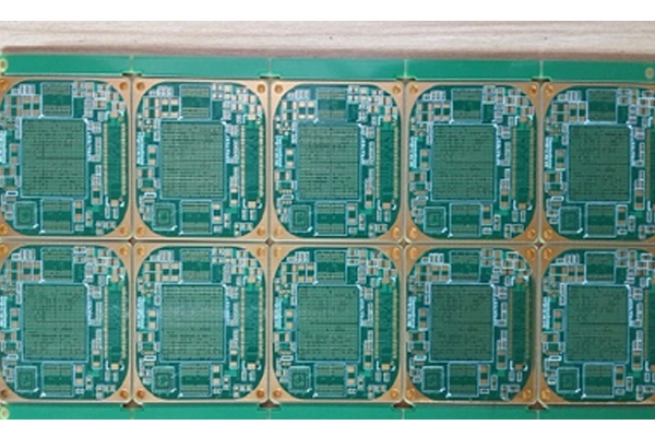
Layer count: 12 HDI PCB
Material: FR4 , 2.0mm, TG 180, 0.5 OZ for all layer
Minimum track: 3.6mil
Minimum space: 3.6mil
Minimum hole: 0.15mm
Surface finished: ENIG
Panel size: 120*268mm/10up
Via on pad PCBs are a specific form of high density interconnect (HDI) PCB which facilitates small form factor designs and superior electrical performance. These PCBs place vias directly in the soldering pads, making routing more efficient and minimizing signal loss, so they are well suited for use in leading-edge electronics, like telecommunications, medical devices and automotive systems. Leaning on the expertise of our skilled professionals, we are able to manufacture a high quality of via on pad PCB that can meet the exact demands of stringent industries.
A via on pad PCB is a sophisticated layout where the vias are located on the component pads. Instead of being positioned away from the component along the board or within the body of the board, the vias are beneath the component itself on the pad. Via on pad technology is particularly useful in HDI PCBs where space is at a premium, and high-speed signal integrity is essential.
Via on pad PCBs are in high demand from consumers and are well known for precision and good quality.
Material Selection
The procedure begins with high-quality material selection used high quality thin dielectric layers and copper foils by the necessary for HDI designs. What makes us different from other PCB manufacturer is that we take the qualified material with good heat resistant and mechanic character for ensuring the strength and long term equipment running.
Laser Drilling for Microvias
Laser drilling is also an essential process in via on pad PCB fabrication. Microvias are formed with high precision laser technology allowing exact location and alignment. This process is necessary to make sure the electrical connections between layers in HDI PCBs.
Via Filling and Plating
Once the through-hole vias have been drilled, they are filled with a conductive material, usually copper, to form a flat surface on which to solder components. Filling removes any voids and non-uniform surfaces that can affect PCB reliability. Following filling, the vias are electroplated to make a robust electrical connectivity.
Pad Preparation and Surface Finishing
The solder pads are modified to be compatible with the via style. Surface finishes like ENIG (Electroless Nickel Immersion Gold) are applied to enhance the solderability of the holes and protect the pads from oxidation. We provide precise surface treatments to enable high-performance applications as your trustworthy via on pad PCB manufacturer.
Testing and Quality Assurance
Through hole on pad PCBs are very well tested. For each via on pad PCB, strong testing is necessary to meet the performance and reliable standard of the industry. That includes electrical continuity tests and mechanical strength.
We provide superior quality via on pad PCB with competitive price on time delivery in a worldwide market. With our experienced engineers and high-end machines, we can guarantee the high precision in each step of manufacture process. We appreciate the complexity of today’s electronic designs and collaborate with our customers to develop tailored solutions to fit their specific needs. From single layer to multilayer via on pad PCB, we have the know how in HDI expertise for better quality.
Via pad PCBs are the backbone of tiny high performing electronic devices and their production requires the know-how of advanced technology. It is very important to select a good via on pad PCB manufacturer to get the best result for your projects. With a strong focus on quality, world class facilities and a wealth of experience in HDI PCB fabrication, we can be your solution for every via on pad PCB requirement.