-
Mail Us Todaysales@efpcb.com
-
Company LocationShenzhen, Guangdong, China
-
+86-755-23724206Call us for more details
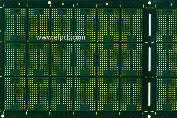
Part No.: E0226060189C
Substrate thickness: 0.22+/-0.03mm
Layer count: 2 layer
Material: SI165
Minimum trace: 80 um
Minimum space: 25 um
Minimum hole: 0.15 mm
Surface finished: ENEPIG
Unit size: 3.76*2.95mm
Integrated circuit (IC) substrates form the basis of today's electronic devices, facilitating connections between semiconductor chips and printed circuit boards (PCBs). The advancement of technology makes a great variety of high performance IC substrates so much in demand, particularly in MEMS (Micro Electro Mechanical Systems) related applications. In this article, in which provides a general introduction concerning the technology of IC substrates, the strength and competitiveness of a leading IC substrates producer are focused.
IC substrates are the critical component between semiconductor dies and PCBs and enable electrical connectivity while also providing mechanical and thermal support. They are critical to the performance and reliability of electronic devices in the consumer, automotive, telecommunications and industrial sectors.
IC substrates are even more important for MEMS devices. MEMS technology combines mechanical structures with electronics, so it requires substrates with superior dimensional stability, fine routing, and thermal capabilities. A reliable IC substrates manufacturer should be able to provide solutions that meet these challenging application needs.
Choice of material: Base IC Substrates
The process starts with material selection. High quality IC substrates are based on sophisticated resin systems, copper foils and dielectric layers. These compounds need to be designed to satisfy rigorous performance requirements such as low signal attenuation, high thermal conductivity and mechanical strength.
One of the premier IC substrates suppliers source the materials offered below:
By tuning their material properties, producers make substrates that not only facilitate the use of high-density interconnects, but that also resist the harsh conditions of MEMS applications.
Fine-Line Circuit Imaging and Patterning
Etching fine-line circuit patterns on IC substrates is one of the most essential process in Substrate Manufacturing. This step creates the complex electrical roadways by imaging and etching copper layers. Ability to produce ultra-fine lines and spaces is known to be one of the most important features of a good IC substrates manufacturer.
The procedure includes:
Applying photoresist over the surface of the substrate.
Employ submicron (micron-level) precision to define circuit pattern through superior imaging processes.
Use acids to etch away copper to make neat, sharp traces.
Fine-line imaging is especially critical for MEMS, a type of technology. Accurate patterns allow high-density routing and compact size solutions for MEMS sensors and actuators.
Via Formation and Metallization
Vias, or vertical interconnections, are necessary to connect multiple layers of an IC substrate, but can be difficult to manage. The via formation process (drilling and plating) requires high precision and reliability.
Leading manufacturers of IC substrates employ state-of-the-art processes such as laser drilling and electroplating to produce microvias, stacked vias and filled vias. These techniques provide:
Dependable electrical connections between layers.
Increased mechanical strength for MEMS support.
Sufficient space for higher-density packaging architectures.
Via integrity is important for MEMS applications. Irregularities in via can disrupt signal paths and decrease the performance of MEMS devices, which is why precision metallization is one of the main differentiators between IC manufacturers.
Surface Finishes for Solderability and Reliability
Surface finishes are applied to the outer layers of IC substrates to protect copper traces and to facilitate robust assembly. Popular finishes are ENIG (Electroless Nickel Immersion Gold), ENEPIG (Electroless Nickel Electroless Palladium Immersion Gold) and immersion silver.
A reliable IC substrates manufacturer customizes surface finishes according to the unique requirements of customers and the resultant advantages include:
Improved solderability for MEMS modules and other high-end packages. Resistant to corrosion for instruments used in aggressive environments.
Long life performance for end use applications.
The surface finish of MEMS devices additionally has to reduce contamination and outgassing for a clean environment assembly process and stable performances.
Dimensional Stability and Warpage Control
As electronic products become more compact, more dimensional stability and warpage control in the IC substrate is needed. Substrates must remain stable and aligned during assembly and operation, particularly for MEMS applications where this is critical.
To this end, producers are refining:
With these considerations in mind, IC substrate manufacturers bring to market MEMS devices that can be trusted to function properly even in the most demanding of environments.
Quality Assurance and Process Control
There must be rigid quality assurance and process control to produce IC substrates for MEMS and other future applications. Tier manufacturers have the following:
These processes guarantee that each substrate attains high standards of robustness and reliability to accommodate the stressed requirements of MEMS applications.
Why Choose a Leading IC Substrates Manufacturer? The quality of the substrates is critical to the performance of MEMS devices and other high-end electronics. An established IC substrates supplier provides:
Specialised knowledge in fine-line imaging and via formation of high-density construction.
Advanced materials specifically MEMS-enabled.
Demonstrated quality – through testing and quality assurance.
Customers that choose to work with a manufacturer who is experienced in the unique MEMS challenges are able to access substrates that not only push the boundaries of what is possible, but that are also able to deliver in the field.
Making the IC substrates is a very sophisticated process that involves the science of materials, precision engineering, and high-end manufacturing. For MEMS, the requirements are even more stringent, demanding substrates with superior dimensional stability, electrical performance and reliability.
A top IC substrates manufacturer that is able to address these needs will help foster the new generation of electronics across different industries. Everything from MEMS sensors to high-speed computing modules depends upon the right substrate to build success in today’s technology-driven world, and nothing builds that success more reliably, or returns to it more consistently, than the right substrate.