-
Mail Us Todaysales@efpcb.com
-
Company LocationShenzhen, Guangdong, China
-
+86-755-23724206Call us for more details
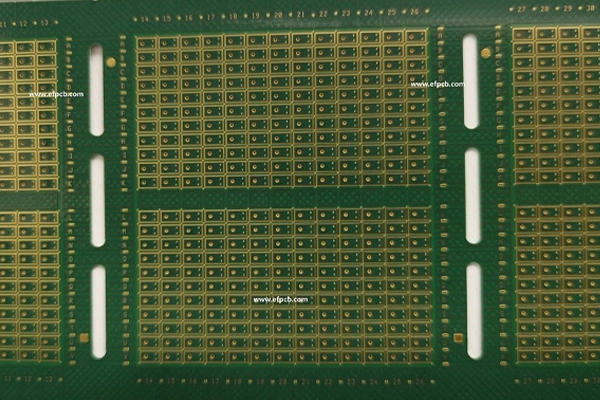
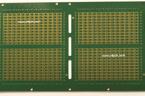
Part No.: E0417060189C
Substrate thickness: 0.25+/-0.03mm
Layer count: 4 layer
Material: BT ( C2006 )
Minimum trace: 220 um
Minimum space(gap): 50 um
Minimum hole: 0.15 mm
Surface finished: immersion gold
Unit size: 3.5*2.65mm
In today's electronics, the IC substrate is the unsung hero: not listed on the product label, but one that dictates performance, reliability, and the extent of miniaturization. For high‑density packaging, 5G and automotive technology, MEMS integration and more, the choice of IC substrates manufacturer is as important as every other aspect of the chip itself.
In this article, you will see the manufacturing process of IC substrates in a state of the art factory and learn the features, both product and processwise, which set a premium supplier apart in markets such as MEMS, high speed computing, and advanced sensing.
IC substrates are the interface between the semiconductor die and the PCB. They enable electrical connectivity, provide mechanical support, facilitate thermal management, and protect against the environment. With increasing device complexity and integration, especially MEMS, the substrate evolves from passive carrier to a key enabler. A leading IC substrate provider must tailor its materials and structures in order to:
Support fine‑line routing for high I/O density Maintain signal integrity at high frequencies Dissipate heat for power‑hungry chips Offer mechanical protection to MEMS devices exposed to vibration, shock, and environment stress For MEMS products (inertial sensors, microphones, pressure sensors), the substrate also provides a precision platform No wonder, these sensors are considered as the heart of any drone, robot, or even your armature application in many electronic circuits. It should have stable dimensions, controlled CTE matching, and robust metallization so that tiny moving structures in MEMS devices remain accurate and reliable over the lifetime of the product.
Core Materials and Stack-Up Engineering
The base of any IC substrate is built upon its core materials and stack-up configuration. A top level process overview at this point in an IC substrates manufacturer’s equipment line might consist of:
High-performance cores: Low-loss resin system, BT epoxy, high speed, high frequency, MEMS compatible advanced organic materials Copper foils: Ultra-smooth copper foils for signal layers with very tight tolerance on thickness for maintaining consistent management of impedance
Dielectric layers: Customized dielectric constant and loss tangent, which is very important RF/HC and accurate MEMS readout
The stack-up is designed to provide the optimal tradeoff among electrical performance, mechanical stiffness, and process ability. Special attention is focused on warpage control and flatness for MEMS, since even minimal amounts of variation can disrupt the MEMS structure alignment and reduce sensing accuracy.
Fine-Line Imaging and Patterning
After the materials and stack-up have been established, the next critical step is circuit imaging. Here the IC substrates producer converts circuit layouts to microscopic copper configurations.
Photoresist Application
Uniform thickness of photoresist layer for accurate line control
To achieve the finest lines and spaces by high resolution imaging
Enhanced etching for crisp, low undercut copper traces!
Today, at such critical processes as fine‑line capabilities to single‑digit microns for leading applications such as MEMS sensor modules and mixed‑signal packages, precision line reduction is more important than ever. This offers the benefit of much larger I/O counts and more compact modules without losing the performance or robustness.
Via Formation and Metallization
Vertical connections are formed by means of mechanical drilling, laser drilling, or a combination. A top tier IC substrates manufacturer will develop and invest extensively in via technology as it has a significant impact on electrical performance and long term reliability! Essential features include:
Microvias for HDI routing and 3D interconnect schemes Stacked and staggered vias for complex multi-layer designs Filled vias to enable routing under pads and advanced assembly
Once drilled, via walls are treated and plated with copper via advanced metallization processes. Via integrity is particularly important for MEMS packaging. Substantial number of MEMS devices need low‑leakage paths and stable resistance as per temperature. Perfect plating of vias contributes to vibration stable sensor performance and uniform signal paths, also under severe operating conditions.
Surface Finishes and Solderability
The surface finishes on the PCBs style of an PCB should be compatible with soldering. External layers of a IC substrate should be the protection, also they can be optimized for the assembly process. Typical surface finishes include ENIG, ENEPIG, immersion silver among others solderable finishes.
Top IC substrates manufacturer reliably customizes surface finish options to specific needs:
Soft gold or ENEPIG wire-bond and flip-chip applications
MEMS modules with low-corrosion finishes for automotive and industrial applications
Finishes to maintain bondable and solderable after Extended Storage MEMS assembly surface finishes also must minimize outgassing, particle generation, and serve clean manufacturing environments while shielding sensitive mechanical features.
Dimensional Stability, Warpage Control and Reliability
As package sizes decrease and more features are crammed inside, mechanical stability becomes a key differentiator. An established IC substrates manufacturer manages all the warpage and dimensional changerelated contributors
Resin formulation and glass cloth selection
Symmetric copper distribution between layers
Profiles of lamination and curing conditions
Post lamination handling and storage
For MEMS devices, this isn’t just a mechanical issue. Warpage and dimensional drift may cause an otherwise perfectly constructed movable structure, optical path, or pressure port to become misaligned, which not only impacts calibration, but also long‑term accuracy. By engineering materials, stack‑ups and lamination processes specifically for MEMS constraints, the substrate is a stable reference platform for MEMS rather than being a source of variation.
Processing Control, Clean Environment, and QA
It is as much about process discipline as it is about the tools to produce high-reliability IC substrates. A high-tech IC substrates manufacturer does business with:
Tight SPC monitoring of critical parameters such as line width and via resistance, layer registration
Inline AOI and X‑ray to identify defects early on.
Cleanroom order of operations in critical stages to allow for MEMS-specific manufacturing
RASS testing, including thermal cycling, HAST, vibration, and mechanical shock
These same practices are vital for MEMS devices destined for use in safety critical applications such as automotive ADAS, industrial automation, medical, and so forth. The substrates are required to support environmental stress, while keeping stable electrical characteristics and mechanical support for the MEMS structures.
Besides of indiscriminate lists of capabilities, customers desire certain product features that make system design simpler and time‑to‑market shorter. Generic differentiators include:
Fine-line capability for high density interconnects in small size modules
High-performance, low-loss and low-warpage RF, high-speed digital and MEMS compatible materials
Custom stack-ups for mixed-signal, power, MEMS and even multiple MEMS technologies in a single substrate
Excellent flatness and dimensional stability for alignment and accuracy in MEMS bonding
Strong surface finishes and metallization to withstand harsh environments and extended life.
In practice, these features enable customers to put processors, RF chips, power management and MEMS sensors on one highly engineered substrate — so they can reduce size and complexity without giving up performance.
The processing of IC substrates assesses a field of materials science, precision imaging, advanced drilling and stringent quality assurance. When an IC substrates supplier brings these techniques to bear on the unique requirements of MEMS and high-density packaging, the substrate becomes more than a passive interposer, it becomes a strategic platform. From consumer electronics to automotive and industrial systems, the substrate vendor you choose subtly impacts signal integrity, reliability, and system miniaturization. For engineers that are pushing the envelope of MEMS integration and advanced packaging, partnering with a manufacturer with a true understanding of IC substrates is one of the best ways to be assured of performance today and preparedness for tomorrow's technology.