-
Mail Us Todaysales@efpcb.com
-
Company LocationShenzhen, Guangdong, China
-
+86-755-23724206Call us for more details
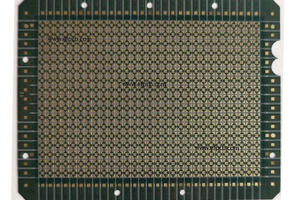
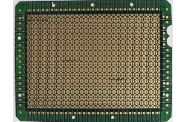
Part No.: E0276060139A
Substrate thickness: 0.11+/-0.03mm
Layer count: 2 layer
Material: SI10U
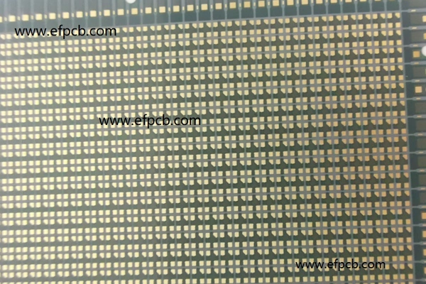
Minimum trace: 180 um
Minimum space: 30 um
Minimum hole: 0.15 mm
Surface finished: ENEPIG
Unit size: 2.3*1.96mm
Brute force The is used to be the gold standard in IC substrate design that you can leverage to meet the standards of today's electronic systems.
When you consider everything from wafer-scale packaging to edge devices, the production route encompasses materials science, surface engineering and high-precision imaging—particularly important for MEMS, advanced logic and RF modules.
In order to design a substrate that will perform under real-world pressure, the very first step is choosing the appropriate materials and defining the stack-up.
The leading IC substrates manufacturer in the industry brings each material to IPC and JEDEC standards, confirming outgassing, reliability under humidity stress, and thermal shock to keep MEMS intact. Patterning & Via Formation of IC Substrate
Controlled photolithography and dry via formation is required for high-density interconnects.
IC Substrate Photolithography: High resolution sub-10 µm alignment accuracy for fine line/space for MEMS signal routing and power delivery.
Laser and mechanical drilling: Microvias (50–75 µm) produced by CO₂ and UV lasers; stacked and staggered solutions for multilayer interconnection.
Desmear and copper activation: Plasma or chemical treatments provide clean via walls and deposit a robust seed layer prior to electroplating.
An established manufacturer of IC substrates will also ensure tight registration and low via resistance, while minimizing crosstalk and thermal drift sensitive MEMS channels.
The quality of the metallization is the critical determinant of electrical performance.
Electroplating: at a capacity for plating on dense arrays uniform copper thickness and maintaining planarity is critical for MEMS alignment and flip chip bumps.
Etching: The edge definition is retained during the etchant controlled-process undercut on the conductor uniformity is limited.
Line/space capability: Down to 10/10 µm for advanced packages, over the entire panel to ensure process reproducibility.
The biological processes are optimized to reduce skew and loss, such that MEMS signals are kept clean even during high frequency operation.
Multilayer substrates are formed by heat and pressure cycles. Sequential lamination: Building up dielectric and copper layers are performed stage by stage to achieve complex stack-ups with buried vias and blind vias.
Resin flow control: Provides void-free infiltration and shields MEMS-related cavities and through-silicon vias from contamination.
Warp control: Balanced stack-up, copper symmetry and customized glass fabrics maintain the panels flat to ensure high-quality panic.
A full-service IC substrates supplier acts on warpage for each panel and lot to ensure MEMS placement and calibration.
Surface Finishes & Assembly Readiness
The final finishing makes the substrate ready for robust interconnects and long term reliability.
ENEPIG: Like noble but suitable for wire bonding, flip-chip and fine-pitch BGA; fantastic for MEMS sensor arrays and hybrid stacks.
A strict IC substrates manufacturer combines statistical process control with full lot traceability for uniform MEMS performance and accelerated failure analysis.
IC Substrate Features That Make Us Unique
Here is a brief overview of the most relied upon functionalities.
Accelerated NPI: Rapid prototypes with the same process window as volume production, speeding MEMS development without compromising quality.
Tighter control planarity, contamination, and electrical noise are required for MEMS than for the usual packages. A specialized IC substrates manufacturer provides:
The production of IC substrates involves precision materials, micro patterning, and rigorous reliability controls: more so for MEMS.
Good IC substrates manufacturer can deliver the performance through disciplined stack-up design, via integrity, low-loss copper and robust finishes.
With an emphasis on MEMS and high-density integration, customers receive stable electrical behavior, clean assembly, and reliable field operation.