-
Mail Us Todaysales@efpcb.com
-
Company LocationShenzhen, Guangdong, China
-
+86-755-23724206Call us for more details
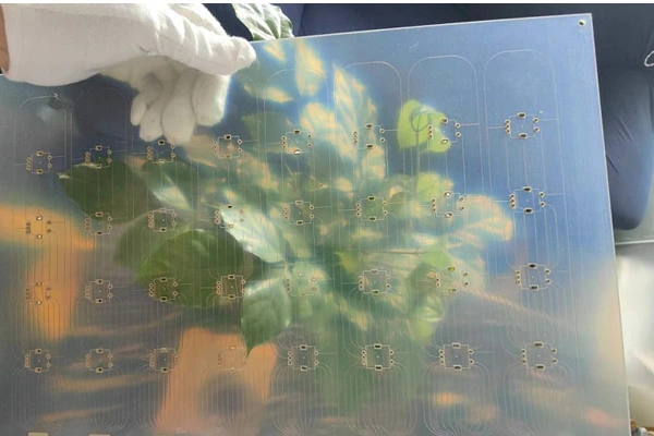
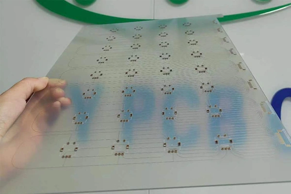
Layer count: 2 layer
Material: Transparent material, 1.6 mm, 1 OZ for all layer
Minimum trace: 400 um
Minimum space(gap): 300 um
Minimum hole: 0.40mm
Surface finished: OSP
Panel size: 250*330mm/1up
Characteristics: Transparent
Modern electronics domain witness innovation that tend to break the barrier on what can be achieved with the circuit design as well functionality. One of the latest avenues happening along with this evolution is Transparent PCBs. Transparent PCBs are quite a huge step ahead, melding with gorgeous and design-oriented possibilities that can make functional luminous interfaces for forward wearable devices to advanced display systems. This detailed guide will get into the specifics of Transparent PCB technology such as materials, production techniques, applications, benefits, challenges and future studies.
Transparent PCB — definition and manufacturing of printed circuit boards with transparency so that light can be transmitted through substrate and conductive layers. Transparent PCBs are different from the conventional PCBs which use black dielectric such as fiberglass for FR4. Instead of glass filler materials with opaque constituent or galvanic barrier for protection Encapsulant witch is being used in traditionally printed circuit boards, Transparent PCBs are manufactured accordingly by placing recently inventible substrates among substrates and conductive resist especially clear as good example. This distinct trait gives genesis to a range of potential options in device architecture, especially for areas requiring high visibility and visual integration with ‘least obtrusive design'.
The transparent PCB technology platform rests in the substrates that are of choice. Glass, quartz, and different transparent polymers (PET — polyethylene terephthalate, polycarbonate PC and polymethyl methacrylate PMMA) are just to name a few common. Among these, flexible transparent substrates such as PET are very popular since they are easier to incorporate with flexible electronics. The substrate should have a high optical transmittance (over 85%) and should be stable over the manufacturing process, working temperature.
Just like in Transparent PCBs, conductive materials is equally crucial when it comes to standard circuits. Standard copper traces are black and not usable for transparent applications. Instead, the Transparent PCB technology utilizes different such as in flour scent materials and indium tin oxide (ITO) which are more porous and can be written on with silver nanowires or graphene conductive polymers. ITO — Being one of the material that boast a good conductivity with transparency, but also very brittle and expensive. The silver nanowires tend to be flexible and show good electrical conductivity but face issues with the oxidation and durability. Graphene—as a single atomically thick layer of carbon—is already being pursued as a promising material for both electrical properties and optical transparence combined with strength, though large-scale fabrication at this stage seems a goal in the far future.
Mass Production of transparent PCBs relies on unique practices to preserve the transparent nature of the materials. While normal PCBs utilize etching to remove the copper layers — which is how one does not produce transparent PCBs, the making of Transparent PCB may use sputtering or chemical vapor deposition (CVD) to put conductive films like ITO on both sides. The patterning of these layers are often done photolithography or take out by ablation processes that predict the items working and do not destroy substrate. Lamination also has to not add bubbles or impurities that can degrade transparency. Roll-to-roll technology refined in this industry has made flexible transparent PCBs possible at scale where critical qualities are consistent along the product length.
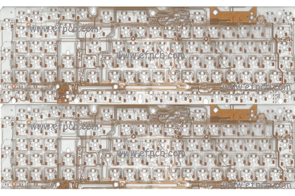
Perhaps the most enticing use case of Transparent PCB technology is in display. Circuitry can be put directly into the viewable area of a display by way of these printed transparent PCBs, which yields the finest in circuit integration and discrete hardware made available as output. Automotive HUDs, for example, use Transparent PCBs to project essential data onto the windshield of a vehicle to help driving safety without being distracting to the driver. Analogously, Flexible Transparent PCBs are responsible for slimmed-down designs in consumer electronics like transparent smartphone and smart glasses where the printed circuit reside within their transparent surfaces. Whereas Transparent PCB technology is best applied in field of wearables. Fitness trackers, smart-watches, and health monitors are quite exacting in their demands when it comes to little parts they should be compact and weightless as well as likely integrated components. Flexible/transparent skin-conforming electronics to request the correct form factor by melding elements seamlessly with a human body is made possible by Transparent PCBs. Its transparency also makes wearables sleek, and users not intimidated by the form of it at all. Transparent PCBs also do a good to not confuse sensors and indicators for its visibility in non-distracting areas by contributing towards the improved user experience.
Transparent PCBs have a lot to offer beyond simply aesthetics from a technical perspective. Their capacity to marry with optical components gives additional great for optical signal integrity in the long run of photonic circuits and sensors. What stand out also is that the lighter and thinner transparent substrates make electronics miniaturization more possible. In addition, Transparent PCBs are also environmentally friendly since some transparent materials make it a possibility for recyclability and actually decreases the overall impact in terms of the adding to electronic devices.
Yet, challenges with Transparent PCB technology are no less significant. The price of materials such as ITOMeanwhile, the complexity of building those layers are the easy part high will drive up on overall production costs compared to conventional PCBs. Another consideration is mechanical robustness as some transparent substrates can be more abrasion prone than say glass. The electrical performance and the transparency must be carefully balanced; in other words, thicker conductive layers result in higher conductivity but less optical clarity. Moreover, transparent components of conventional electronics are necessary to be implemented with innovative packaging and interconnection solutions for reestablishing transparency along the device.
The statistics and numbers within the industry testify to the fact that Transparent PCB technology becomes more and more significant. This means that according to MarketsandMarkets Report, the world-level transparent electronics market (which includes all kinds of Transparent PCBs) is poised to deliver nearly 20% CAGR from 2023–2030. This momentum is driven by higher demand heading future sectors such as consumer electronics, automotive, healthcare and aerospace. There is heavy money pouring in currently from leading form factor electronics companies as well as think tank houses all over today to get at your current limitations and tap into what is possible with transparent PCBs.
Summary of the future of Transparent PCB technology ahead. Nano materials and printing technologies are going to lower the cost, all while weaning us off Screen Printing for scalable sheet materials. For example, we have been able to build hybrid conductive inks that combine silver nanowires and graphene which could provide the material foundation for next generation Transparent PCBs with exceptional flexibility & durability. There are further expansions in new dimensions to be found with the integration of upcoming technologies such as flexible batteries, micro-LEDs and even transparent sensors. Plus, a trend toward greener electronics matches the use of eco-friendly transparent substrates and recyclable conductive materials.
Ultimately placing, Transparent PCB technology is a major milestone in the evolution of electronics design and manufacturing. Transparent PCBs make possible functional circuits that are visually unobtrusive with multiple applications across industries. Though there are costs still to be worked out with regard to longevity, durability and integration, the momentum of the research and market suggests that Transparent PCBs will be more than just simply next but in fact even mainstream. In becoming competent, this technology gets to reinvent how we think electronics develop, with a combination form and function never seen before. The evolution of Transparent PCB technology from exotic usage to mainstream applications with dedicated developments through material science, fabrication techniques and design methodologies. Those are important for engineers, designers and manufacturers to get some basics knowledge about the scale of opportunities available with the Transparent PCB technology. This is a primer for all who want to learn deeper or start working with Transparent PCBs, dive in and read around all the important take-a-wins that await.