-
Mail Us Todaysales@efpcb.com
-
Company LocationShenzhen, Guangdong, China
-
+86-755-23724206Call us for more details
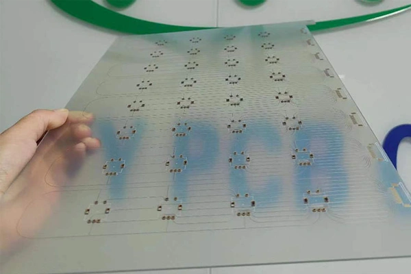
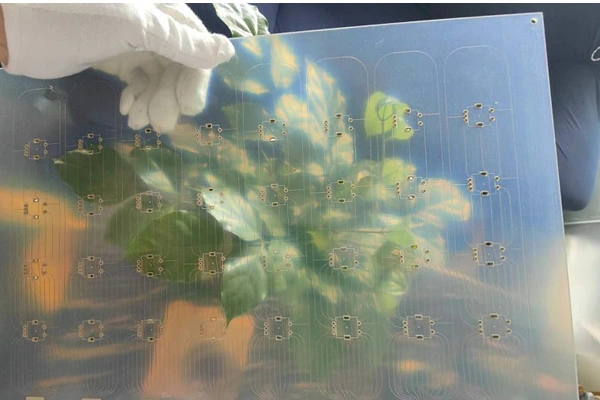
Layer count: 2 layer
Material: Transparent material, 1.6 mm, 1 OZ for all layer
Minimum trace: 300 um
Minimum space: 300 um
Minimum hole: 0.40mm
Surface finished: OSP
Panel size: 230*380mm/1up
Characteristics: Transparent
The rapid evolution of electronics field has stirred a number of research and development projects in pursuit of original circuit solutions: functional but also unique aesthetics. One of these innovations, Transparent PCB stands out as a revolutionary technique due to its ability to seamlessly combine performance attributes with appearance transparency. This technology specifically targets applications where beauty is equally if not more important as functionality, such as consumer electronics, wearables or decorative lighting. This tutorial intends to delve into the nitty-gritties of Transparent PCB technology, materials, manufacturing using a state of the art process, different features and contributive areas that have used and would in the future use this technology in distinction from end users.
Understanding what defines a transparent PCB is pivotal to get the idea of it. Different from common PCBs that are transparent due to the layers being printed on and substrate materials Abstract systems, Transparent PCB is to use light (also referred to as the infrared at that time) in order for the structures below it to come into view. Through the use of certain materials and innovative fabrication techniques that either mask or make conductive and dielectric layers invisible.
Get informed about the core concept from Transparent PCB technology is to swap standard opaque materials with clear or slightly opaque materials. Polyimide, for the dielectric layer, Polyimide-based transparent PCBs can be used in environments of high temperatures and limited mechanical stresses as polyimide is very robust. These materials offer an exceptional optical clarity and suitable electrical properties. The conductive layers where it is appropriate, use ITO like indium tin oxide (ITO) or nanowires of silver with transparent conductive polymers. Such materials do not lose their electrical properties but allow light to pass through them, which is useful if the end goal of your product is transparency.
Polyimide is a mainstay in the fabrication of Transparent PCB, an incredibly thin film material with phenomenal thermal stability, flexibility and optical clarity. Polyimide based transparent PCBs can be used in applications that require high thermal mass and mechanical constant. When combined with transparent conductive materials such as ITO or silver nanowires, these PCBs can show excellent electrical performance while maintaining transparency.
The manufacturing of Transparent PCB involves many critical steps. The first step is to prepare a transparent substrate-based off-the-shelf material such as a polyimide film. Next, the transparent conductive layers are deposited using sputtering, chemical vapor deposition (CVD) or inkjet printing. This could offer more accurate control over the thickness and uniformity of the conductive layer. The conductive layer is then patterned with photolithography or laser ablation that decides on the exact circuit paths. The circuitry can be protected by additional insulating layers, to keep its transparency at the same time.
The chief difficulty in fabricating Transparent PCB is maintaining a balance between electrical conductivity and optical transparency. Especially conductive materials like ITO which is amongst the most transparent are brittle and this can make them costly thus making it mainly unsuitable for mass production. Silver nanowires and conductive polymers present more flexible, but also all too often with clever deposition techniques and surface-treatment required to match their stable conductivity and bond.
Transparent PCB technology has its own set of advantages, which makes it a paragon in applications with a concrete point of use. It can be used in a pretty clean form of aesthetics: transparent circuits can be embedded in devices where the inside components should be exposed to give more visibility and clarity to the device overall. This is especially important in consumer electronics where the internal components being visible can be an element to the design or wearable technology which appearance of hints from transparency. Which sets in perspective a very important advantage is the optimization of device integration toward miniaturization. What Transparent PCBs provide the designer, in short is the ability to create multi-layer assemblies with in a systems visible to the naked eye. This might make the product we design, be more exceptional and awe-inspiring by way of see-through displays or even devices lit and with circuitry inside embedded in the casing form circuits that we can see.
It also improves thermal management in these transparent PCBs, notably coupled with ITO thin films that are an ideal thermally conductive material but lack high thermal stability. They are used in automotive lighting, medical elements and high power electronics that require to run reliably at the extremes of performance.
What is more, by being transparent PCBs, we can provide options for optical and optoelectronic devices as LEDs, solar cells, or sensors. Their ability to conduct light enables integrated optical functionalities and electronic capabilities in devices that has only recently become possible.
Though transparent PCB technology looks promising it has many hurdles to overcome. The biggest hurdle in realizing high performing, conductive PCBs with 92% of the original transparencies comes down to electrics. Effective Technologies like ITO are expensive but have low transparencies are hard, therefor they have meaningful applications in practice.
Conductive polymers and nanowire-based conductors on the other hand are promising, but often demand for complicated fabrication methods and surface treatments to be stable over long time scales.
Another major consideration is durability and environmental stability. As transparent PCBs are more sensitive to the environment—inhaling and UV exposure both ways will degrade optical performance as well as electrical performance. These unwanted issues are often addressed with protective coatings and encapsulation techniques but this usually adds complexity and cost to the manufacturing process.
In addition, the fabrication of transparent circuits with high accuracy and repeatability is still a technical problem. Explore some of the latest techniques, such as laser ablation, inks jet printing and nano imprint lithography, that are providing improvements in patterning resolution and scalability.
These approaches will also get better over time which will increase the cost-effectiveness and commercial viability of transparent PCB.
Transparent PCB Applications are endless and wide-ranging across multiple industries. For consumer electronics — transparent circuits are used in smart, stylish displays and touch screens — tying aesthetics with functionality. In automotive lighting and displays, the use of transparent PCBs allows for very clean and integrated designs with an emphasis on vehicle aesthetics and in-display user experience.
Implantable electronics and diagnostic devices, as well as biosensor research and development all fall under the category where the ability to see and biocompatibility are vital for transparent PCBs to be used in applications. The architecture of these devices with the transparent components lowers both realization and integration complexity– optical component are easily integrated in.
In the realm of smart packaging and IoT devices, embedded transparent PCBs can be integrated into various packaging materials to deliver an uncompromised visual perspective while also creating seamless connectivity and data capture.
What is the outlook for Transparent PCB technology? The future of Transparent PCB technology rests on new developments in materials science, fabrication process and ways to integrate devices.
A wide array of transparent conductive materials with enhanced electrical properties are being investigated by researchers, allowing for more transparent and flexible electronics that work under many environmental conditions. For example, graphene conductive films can potentially be suitable as it has very high electrical and mechanical performances. The future of transparent PCB fabrication is expected to be one of additive manufacturing and printing technologies that can undergo quick prototyping as well as cost-effective large-scale production with highly integrated circuits able to fulfil dimensionless scaling. They are ways of lowering the price and offering custom made transparent electronics to be more available for different types of businesses.
Further, the domain of applications for Transparent PCB will be extended even more using integration to related emerging technologies such as Flexible electronics, Stretchable devices and Wearable systems.
As the demand for electronics with beautiful appearances and high performance continues to rise, so will the importance of transparent circuitry.
So in short, the transparent PCB technology is an interface of electrical engineering, materials science and design creativity. The electrical and optical functionality in one can only be done by this material, and there are new kinds of applications that we will be able to do with our appeal devices in electronic devices that are visually rich and conveying performance. There are challenges existing but with ongoing research and technology progress the limitations will be solved and adoption will improve or new application domains.
Electronic device design is advancing where electronic companies have been squeezing new capabilities into the next evolution of device form factor, and Transparent PCB will play an important part in creating a future for transparent, intelligent and look-new electronics. The promise of a change in the way products look and work is very amenable territory for research and development — and commercialization.