-
Mail Us Todaysales@efpcb.com
-
Company LocationShenzhen, Guangdong, China
-
+86-755-23724206Call us for more details
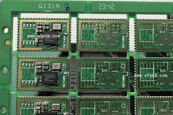
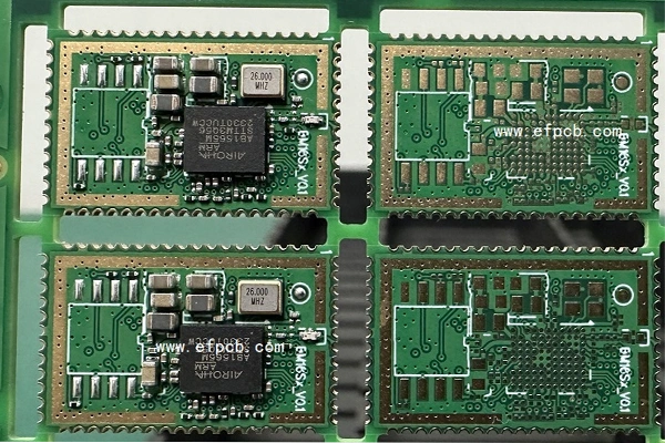
Layer count: 6 Layer HDI PCB
Material: FR4, TG170 , 1.6 mm, basic copper 0.5 OZ for all layer
Minimum tack: 2.5 mil
Minimum space(gap): 2.5 mil
Minimum hole: 0.15mm
Surface finished: Immersion Gold
Panel size: 120*138mm/20up
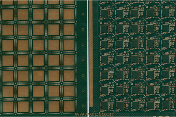
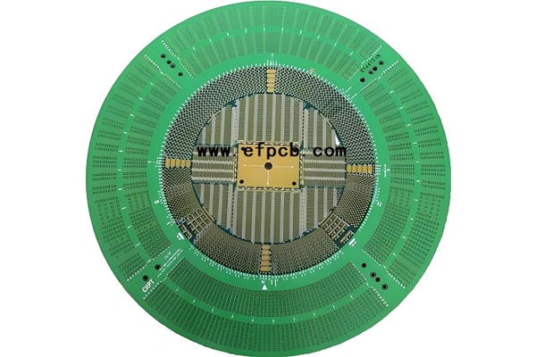
Characteristics: 0.17mm BGA ball size, 0.35mm pitch BGA PCB assembly, high density interconnect PCB, via on pad(plug with resin, copper capping), high TG, thin core 3mil thickness
Small pitch BGA PCB packaging introduction to BGA or Ball Grid Array technology is one of the latest electronic packaging solutions where the whole IC (Integrated Circuit) size is packaged without any lead using solder balls. With the increasing miniaturization and power of electronic devices, the need for small pitch BGA PCB assembly has increased dramatically over the years. This high-end assembly technology is vital for Applications that require precision, reliability and effective thermal management. In this post, we will look at the manufacturing, product features and significance of small pitch BGA PCB assembly in modern electronics.
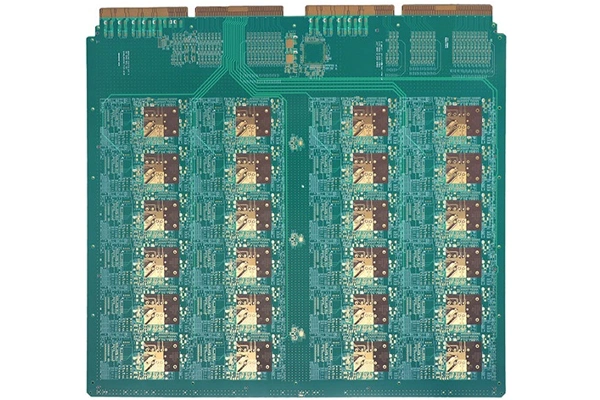
Small pitch BGA means that the distance between the solder balls of the ball grid array is smaller and the distance is less than 0.8mm usually. This results in higher component density and smaller package sizes, making it particularly suitable for small devices like smartphones, IoT devices, & wearables. The process of small pitch BGA PCB assembly has a following bearing: position these parts and soldering them on a printed circuit board, have got electrical and mechanical connection.
1. PCB Design and Preparation
The process starts with creating the PCB layout for small pitch BGA components. The trace routing, via placement and pad design is all optimized using advanced CAD tools for high density interconnections. Then the PCB is made from a material that allows good thermal and electrical performance.
2. Stencil Printing
Apply the solder paste stencil to the PCB. To be done properly enough paste to be deposited with an equal amount on each pad. Fine-pitch stencils are used for small pitch BGA PCB assembly to fit with smaller pitch between the solder balls.
3. Component Placement
BGA components are placed on the PCB with precision by automated pick and place machines. These machines now contain sophisticated vision systems to work with the tiny pitch BGA packages.
4. Reflow Soldering
The PCB is run through a reflow oven, which causes the solder paste to flow, makin dependable connections between the BGA balls and the PCB pads. Temperature profiles are tightly controlled to avoid thermal shock to the parts.
5. Inspection and Testing
After soldering, the assembly is inspected thoroughly using X-ray machines not only to check whether the solder joints are intact. Also, electrical tests are run to check functionality and signal integrity.
High Density Interconnections: The smaller component size and tighter spacing contribute to high-density interconnections, which can be used to develop compact product designs.
Efficient Thermal Management: Optimized board layout and solder joint robustness allow efficient heat transfer.
Improved Signal Integrity-Chip: Socket and pin interface are minimized and precision aligned to reduce electrical impedance and noise.
Scalability: Designed for multi-layer PCBs and complex layouts, so are suitable for high performance needs.
Performance: Strict quality control and testing guarantee long-lasting stability and performance.
Featured in modern manufacturing, the small pitch BGA PCB assembly has been essential in the rise of miniaturized electronics. The global PCB assembly market is anticipated to reach $ 71.3 billion by 2026 owing to the growth in packaging technologies such as ball grid array as per a report by MarketsandMarkets. This technique of assembling is vital to industries like consumer electronics, automotive, space, and medicine where small and reliable designs are a necessity.
What is small pitch BGA PCB assembly?
Smaller pitch BGA PCB Assembly is the surface mount technology for mounting of BGA packages with reduced pitch (<0.8mm) on PCB. It finds application in high-density and compact configurations. Why is small pitch BGA assembly difficult?
The closer spacing between solder balls makes accuracy in alignment, the use of more advanced equipment and the application of more stringent inspection protocols a must to achieve reliable connections and prevent defects such as bridging or voids.
What industries are suitable for small pitch BGA PCB assembly?
Small pitch BGA assembly is used in consumer electronics, automotive, aerospace, and medical applications for small high performance.
How to confirm solder joint integrity in small pitch BGA PCB assembly?
Solder joint quality is checked with x-ray inspection and electrical test to verify reliable connections. A good reflow soldering profile will also reduce the amount of defects.
Can you do small pitch BGA PCB assembly for multilayers?
Yes, small pitch ball grid array assembly can be used with multilayer PCBs. complex designs for high performance applications.
The tight lead spacing in small pitch BGA PCB assembly is a key technology for modern electronics, which not only allows a high density interconnected chip but also can reduce the volume of integrated chip. With the integration of latest manufacturing technologies and exhaustive testing, this mounting technology delivers dependable operation and scalability for numerous applications including automotive, industrial and consumer. As the trend toward even smaller and more powerful devices continues unabated, small pitch BGA PCB assembly is at the leading edge of electronics industry evolution.