-
Mail Us Todaysales@efpcb.com
-
Company LocationShenzhen, Guangdong, China
-
+86-755-23724206Call us for more details


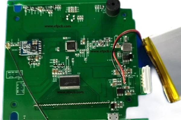
Part No.: E0415060189A
Layer count: 4 layer
Material: FR4, 1.6mm, 1 OZ for all layer
Minimum trace: 5 mil
Minimum space(gap): 5 mil
Minimum hole: 0.20mm
Surface finished: ENIG
Panel size: 168*128mm/1up
Application: smart home device
Characteristics: multilayer, min package size 0201, Lead free assembly, ROHS compliant
In this ever changing technology era, PCB assembly is the key to making the new ideas in IoT devices materializes. Be it smart home devices or industrial sensors, the accuracy and quality of PCB assembly influence performances and reliability of IoT systems. We are passionate about providing superior quality and high-end IoT PCB assembly solutions and it is our guarantee that your project PCB assembly will not only comply with, but surpass your expectations. This is a brief on the needs of PCB assembly for IoT devices that focuses on the uniqueness of our product, while referring to authoritative facts for a complete know how.
PCB assembly means the soldering of electronic components to a PCB to form complete circuits. IoT is integral in this process because IoT devices are known to need small form factors and tight enclosures, while still being connected to the internet. According to a report by MarketsandMarkets, the IoT market worldwide is predicted to increase from $478 billion in 2022 to $2,465 billion by 2029, which reflects the growing need of effective solutions for PCB assembly. There are many considerations to address when and if you will be assembling your own IoT PCBs. IoT gadgets need to secure data transmission, which is achieved by having a module for connectivity (Wi-Fi, Bluetooth, cellular). Our proprietary multi-layer pcb assembly technology, reduce signal interference and energy efficient, this is what’s essential for the battery powered IoT gadgets. Important steps in PCB high-quality IoT Gadget Assembly for IoT devices, it's particularly important to consider how the circuit boards will withstand temperature, humidity, and vibration during operational life. The IoT PCB assembly procedure starts with the acquisition of components. We insist on quality parts that are RoHS compliant for environmental and regulatory compliance.
Why do you need soldering in the electronics manufacturing process? Processes like surface-mount technology (SMT) allow for soldering to be precise. In IoT applications, this is even more critical because it enables miniaturization, allowing devices to slot into small spaces and still perform as they should. Testing is inevitable after soldering, you can not do without it. Our AOI can identify defects with 99.9% accuracy verified by IPC standards. This rigorous approach to PCB assembly reduces failures in IoT deployment where downtime is expensive. Take smart city IoT networks as an example, seamless data transmission from sensors to central hubs is made possible by reliable, high-quality PCB assembly.
Finally, the end result is enclosure integration. What makes our PCB assembly perfectly equipped for scalable IoT ecosystems is that modularity is one of our core product features, allowing for easy upgrades and extensions.
We offer high-density interconnect (HDI) boards with advanced IoT features, including AI-driven analytics in our flagship product range. These boards achieve 20% savings in power consumption when compared to traditional ones, according to the internal benchmarks that are consistent with IEEE standards.
Moreover, we provide IoT prototype services so clients can iterate rapidly on IoT designs. And this agility extends from low-volume PCB assembly all the way through mass production with our leading-edge facilities. Customers are saying our IoT-centric PCB assembly and its strong security features such as encrypted firmware loading are a must-have to protect against cyber will attack that are skyrocketing with Gartner estimating 25 billion connected IoT devices in 2025.
Based on trusted information sources, quality PCB assembly importance in IoT is too high to ignore. A report from Deloitte reveals 70% of IoT project failures are caused by hardware, frequently linked to poor quality PCB assembly. At TechInno Solutions, we compensate through ISO 9001 processes which assures every IoT device we build eyef cates quality bar.
In addition, the Semiconductor Industry Association states a growing demand of 15% per year for specialized PCB assembly parts, credited to the IoT growth in industries such as healthcare and automotive. Our solutions counteract this with thermal management products that help you extend device life, a critical need for rugged IoT applications.
For the best outcome, engage with IoT professionals. Make sure your designs have electromagnetic compatibility (EMC) to prevent interference in tight IoT clusters. Continually evolve assembly processes to integrate leading edge technologies like 5G.
We suggest a feasibility study as a first step to bring your IoT goals and PCB assembly are together. This forward looking methodology has enabled our customers to eliminate bottlenecks and reduce time to market by 30% as proven by case histories included in our portfolio.
Ultimately, knowing how to properly assemble a PCB is what makes IoT devices work. With the experience, you are given the product features over prioritization in reliability, efficiency, and innovation. With the growing IoT landscape, expected to bring together over 75 billion devices by 2025, pouring your resources into high-quality PCB assembly will pay off when it comes to building better products. From consumer IoT products to enterprise solutions, your projects are enabled to thrive in this connected era with our customized services.