-
Mail Us Todaysales@efpcb.com
-
Company LocationShenzhen, Guangdong, China
-
+86-755-23724206Call us for more details
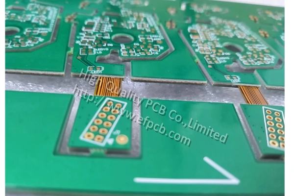
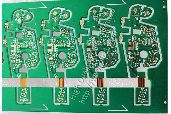
Layer count: 8 layer
Material: FR4, 1.6mm, high TG +2mil PI, 1 OZ for all layer
Minimum track: 4 mil
Minimum space: 4 mil
Minimum hole: 0.20mm
Surface finished: Gold plating PCB
Panel size: 228*128mm/6up
The demand for rigid flex PCBs solutions in the electronics industry has been growing tremendously and industry research forecasts the global market to be around $2.3 billion by 2027. These high-performance circuit boards offer a combination of the rigid boards stability and robustness with the flexible circuits versatility and flexibility, thus can be found in modern electronic applications ranging from mobile phones to aerospace applications.
To know how to make rigid flex PCB, you need to understand the sophisticated techniques based on many different processes, and production process are significantly different from those of standard PCB production. They stated that "Each manufacturer involved with this specialty technology must develop unique processes to produce their own product that can satisfy the challenging performance requirements while being cost effective.
Rigid flex PCB technology is a hybrid method in which rigid areas retain standard board characteristics with mechanical support and component packaging while flexible areas allow 3D packaging and dynamic flexing. This special design enables engineers to completely avoiding connectors, minimizing assembly time and enhancing system-wide performance.
The challenge in fabrication lies in the tight integration of dissimilar core materials and process conditions within one single board. According to the data collected from the industry, the applications of rigid flex PCB had been increasing at a rate of 15 percent per year, which was mainly led by miniaturization of technology in consumer electronics and automotive industries.
Material selection is dependent on key properties. Owing to their exceptional thermal stability and mechanical properties, polyimide films with a thickness of 12.5‐125 μm are used as a flexible substrate. For rigid layers, the material of choice is usually the FR-4 epoxy resin which is the standard material used in the majority of PCBs.
Copper foil choice affects performances. But, What Does Copper Foil SMOOTH and ROUGH REALLY Mean Annealed copper Rolling and annealing a copper foil sheet with a thickness of 9 to 70 microns make it softer and more ductile superior to electrodeposited counterparts. Standard electric and aluminum lead applications.
Thermosetting adhesives are applicable to bond layers and remain unaffected through temperature cycles from -55°C to +200°C. Acrylic and modified epoxy adhesives are widely used and the manufacturing companies formulate proprietary products.
Development and Engineering Stages
Starting the production process with extended design rule checks (DRC) to verify on manufacturability, the processing path is defined by the process and material properties. Engineers must consider bend radius requirements, which are usually a certain minimum ratio of the cable diameter e.g. 6:1 for dynamic applications and 3:1 for static application. Simulation software can now also be used to predict areas of high stress and possible failure.
Layer stack up preparation defines final board attributes. Rigid flex PCB stack up can range from 4-12 layers, with flex areas made up of 1-4 conductive layers. Each manufacturer has individual rules for via spacing, trenching, and routing traces in transition zones.
Drilling Operations
Precision drilling is a hallmark of manufacturing. Mechanical drilling is used to drill larger holes and vias, laser drilling is used to drill microvias with diameters as small as 50 micrometers. Statistical process control (SPC) data from leading drilling facilities indicate accuracies in drilling of ±25 micrometers for standard operations.
Unique polyimide drill bits ensure no delamination and clean hole wall. The drilling order has to be adjusted to the differences between materials, i.e. rigid section are drilled with normal speed and feed rates, flexible with different ones.
Lamination Process
Lamination is the process of converting layers into a rigid flex PCB. The process requires fine control of temperature and pressure typically at 170-200°C with 200-400 PSI of pressure. The length of the lamination cycle ranges between 60 and 120 minutes based on complexity of stack up.
Sequential lamination processes enable fabricators to progressively fabricate high density interconnect (HDI) structures, such as blind vias and buried vias, which place less strain on flowable materials. Vacuum press lamination extracts the air from between layers, allowing uniform bonding between adjacent board layers within the whole laminated panel.
Imaging and Etching
Circuit patterns are defined by photolithographic processes with incredible accuracy. Handling equipment for applying dry film photoresist to flexible substrates must be designed to transport the material without inducing wrinkles or trapping air. Exposure systems must be designed to handle different substrate thicknesses in the rigid and flexible sections.
Selective removal of undesired copper while retaining circuit traces. The optimized etchant chemistry ensures homogeneous dissolution rates for different types of substrates. Well-made PCBs can tolerate a trace width deviation of up to 10% of its nominal value.
Plating and Surface Finishing
Electroless plating is employed to deposit a thin layer of copper in the drilled holes and over the surface features. The control of the current density is also very important in rigid flex PCB manufacturing, the reason for that is the varied conductor patterns and varying substrate material on these assemblies. Typical plating thickness of 20-40 μm (typical plating thickness of through-holes).
Surface finishing solutions include ENIG (Electroless Nickel Immersion Gold), HASL (Hot Air Solder Leveling), and OSP (Organic Solderability Preservative). All finishes have different benefits, however ENIG has exceptional solderability and corrosion resistance for high-reliability application. Quality Control and Testing
Electrical Testing
The electrical integrity and functionality of circuits are confirmed by full electrical testing. The automated test equipment (ATE) for continuity, isolation, and impedance testing. 100% elctricial test is needed according to industry's standard if rigid flex PCB product for critical application.
In-circuit testing (ICT) and flying probe test can be used to test rigid flex PCB. The test fixture design has to consider the flexible parts and also provide good electrical contacts.
Mechanical Testing
Flexibility test confirms the flexible part is robust in its use environment. Standard testing protocols are based on bending angles/frequencies within the application. Typical specifications are survival 100K to 1M bend cycles depending on the application.
The peel strength determines the adhesion between layers and good values are generally higher than 1.0 N/mm for rigid to flex transitions. Environmental testing subjects assemblies to temperature cycling, humidity exposure, and thermal shock.
The rigid flex PCB manufacturing supports new technologies including embedded components, blind and buried vias and HDI (High Density Interconnect). These enhancements require special tools and processing skills that can be only found from a lead provider of manufacturer services. Advanced rigid flex designs can reduce total system volume by 60% over traditional rigid board solutions mated together with cable interconnections, according to statistics from the industry leaders. This space saving continue to boost adoption in a variety of application and market.
Rigid flex PCB technology requires an excellent accuracy, special equipment and a huge know-how regarding process. The best performance and manufacturability of a flex circuit can be achieved through close cooperation of experienced manufacturing teams and flex design engineers. With electronic systems moving increasingly toward smaller size and with more features, rigid flex PCB solutions will become an increasingly critical element in developing next generation products.