-
Mail Us Todaysales@efpcb.com
-
Company LocationShenzhen, Guangdong, China
-
+86-755-23724206Call us for more details
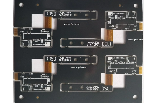
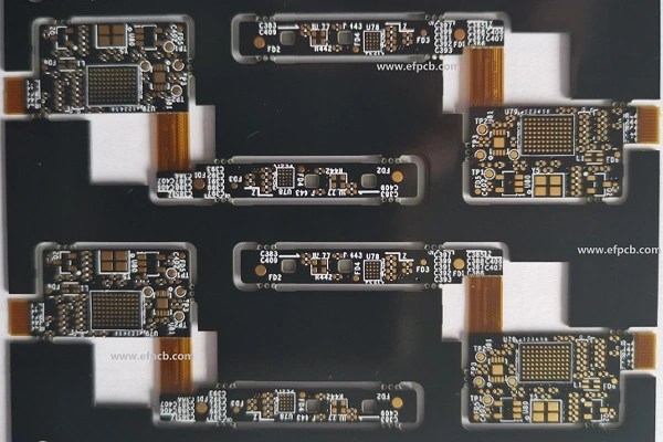
Layer count: 4 layer
Material: FR4 IT180A, high TG +1mil PI, 1.00mm, 1 OZ for all layer
Minimum tack: 3.5 mil
Minimum space(gap): 3.5 mil
Minimum hole: 0.20mm
Surface finished: ENIG
Panel size: 128*148mm/4up
The versatility of the flex circuit, combined with the growing complexity of today' s electronics, has leaded to an increased demand for rigid flex PCB with impedance control. Such state of the art stack-ups are indispensable for high frequency applications, such as 5G communication devices, IoT systems and medical equipment where signal integrity is paramount. To successfully achieve tight impedance control in rigid flex PCB manufacturing, it is essential to have a detailed understanding of the material and manufacturing processes, as well as design optimizations. In this article, we will go through the step by step process of manufacturing an impedance control rigid flex PCB and along the path, highlighting the important points for manufacturers.
Impedance control is the maintenance of consistent electrical impedance in the transmission lines of a PCB. In high-speed circuits, signals are traveling at frequencies where mismatched impedances producing reflections, signal loss, radiating EMI and causing signals to EMI.
Rigid flex PCBs provide the excellent mechanical protection pick of rigid PCBs while adding the versatility of flex PCBs which makes them ideal for applications that need impedance control and other critical requirements. Manufacturers have to make sure that the impedance of trace within the PCB is tightly matched to the requirements of the system, and this is normally done through proper material selection, stack-up design, and process control.
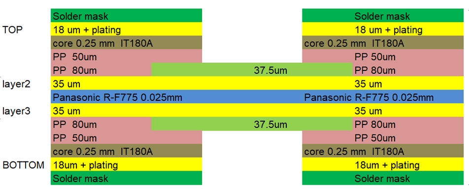
Substrate Materials
Material choice is the basis for impedance control in rigid flex PCBs. Manufacturers usually apply polyimide for the flex layers because of its superior electrical characteristics and thermal stability. Rigid layers are normally constructed of FR4 material, but for high frequency applications, low loss materials such as Rogers or PTFE may be necessary.
The Dk and Df of the materials have a significant impact on the impedance. For example, the lower the Dk, the faster signals propagate and the lower the Df, the less signal loss. It is well understood that Dk in the range of 3.0 to 3.5 is common place for impedance-controlled designs."
Layer Stack-Up
The layer stack-up design is a vital element in achieving impedance control. Producers need to precisely specify the rigid flex layers, the number of signal and ground layers, and the thickness of dielectric materials.
Constrolled trace geometry: How traces' width, thickness (height), and spacing affect impedance.
Reference planes: Signal layers are stacked with ground or power planes to provide uniform impedance.
Dielectric thickness: The distance between the signal layer and the reference plane should be adjusted in order to satisfy the impedance requirements.
Simulation tools (e.g. Ansys, polar SI9000) are extensively applied to simulate and predict the impedance in the stage of designing.
Pre-Production Stages
The rigid flex PCB design is reviewed stringently before production in order to satisfy impedance specifications. Industry leading software is employed for calculating trace/wire widths, spacing and stacks.
After the design is complete, photo tools are made for each layer. These photo tools will be effectively used in the imaging and etching procedures to have the exact trace patterns.
Imaging and Etching
The imaging separates circuit patterns on copper layers. A dry film photoresist is laminated on the copper, the wanted trace patterns are exposed by UV.
Once the PCB is imaged, the exposed copper is etched chemically, then what was left is the traces that makes the circuitry for that PCB. And the manufacturing process should be closely controlled at this stage of production, because small changes in trace width and spacing can affect the impedance.
Lamination
The rigid and flexible layers are laminated (bonded together) in a rigid flex PCB with the use of heat and pressure. In impedance control, the manufacturer should maintain a uniform dielectric thickness between layers, because non-uniformities may result in impedance mismatches.
Sequential lamination is typically employed for multi-layer complex patterns. To each lamination cycle must be watched with the eye of a hawk to avoid distortion or shifting, which could lead to impedance changes.
Drilling and Plating
After lamination, holes are drilled for vias and through-hole components. To achieve excellent quality, traditional mechanical drilling and laser drilling are used together, especially when microvias are drilled in high density designs.
First, plating is carried out to deposit a thin layer of copper on the wall of holes to establish electrical connection between the different layers of the hole. The thickness of plated copper must be accurately controlled, and it can affect the impedance of the transmission line.
Surface Finish and Solder Mask
Copper traces are protected from oxidization and a surface finish enhances solderability. Typical finishes used in impedance control rigid flex boards are ENIG (Electroless Nickel Immersion Gold) and immersion silver, which provide a flat surface and predictable performance for high frequency signals. An insolation solder mask is then placed over the traces to keep them insulated from one another and to prevent solder bridging during assembly. There must also be no effect of the solder mask on the impedance of the controlled impedance traces.
Testing and Quality Assurance
Impedance Testing
To test that the rigid flex PCB meets the requested impedance, manufacturers' test on rigid flex PCB by Time Domain Reflectometry (TDR) or Aerospace network analyzer. These instruments sample the impedance of the transmission lines and locate where impedance mismatches or reflections may occur.
Electrical and Mechanical Testing
Along with electric testing for impedance, the rigid flex PCB is tested electrically for continuity and for failures such as shorts or opens. They also undergo bend testing to determine whether the flexible areas can resist recurring bending without having an effect on the functionality.
Industrial standards must be met on the part of the manufacturer, e.g. IPC-6013 for rigid flex PCBs, or IPC-2141 for impedance control. They provide specifications for the materials, design, and test procedures enabling dependable performance in high stress environments.
Problems of impedance controlled Rigid Flex PCB production
To have a finely controlled impedance on rigid flex PCB is not an easy work and need high knowledge and advanced facility equipment. Some of the key challenges include:
Material variability: Differences in dielectric properties between stiff and flexible substrates may pose problems for impedance control.
Trace geometry: Keep trace width and spacing uniform over the rigid and flex portions.
Process control: Etching, lamination and plating process variations can cause impedance variation.
To address these challenges, it is important to work with a proven manufacturer with expertise in impedance control rigid flex PCB fabrication.
The market for impedance control rigid flex PCBs is expanding at a fast pace as the industries are reaching the maximum limit of high-speed and high-frequency electronics. The making of these sophisticated boards requires careful consideration of material selection, design, and process controls the manufacturing of these advanced boards takes place:
By partnering with expert manufacturers, organizations can make sure their rigid flex PCBs adhere to the high bar for signal integrity, reliability, and performance.
When approached correctly, impedance control rigid flex PCBs have the potential to gallop in uncharted new ground applications leading to smaller, faster and more efficient electronic devices and so on.