-
Mail Us Todaysales@efpcb.com
-
Company LocationShenzhen, Guangdong, China
-
+86-755-23724206Call us for more details
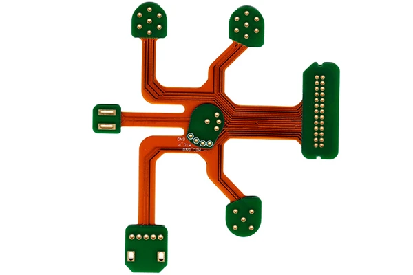
Part No.: E0415060179A
Layer count: 4 layer
Material: FR4 TG170, 1.6mm, high TG +2 mil PI, 1 OZ for all layer
Minimum track: 5 mil
Minimum space(gap): 5 mil
Minimum hole: 0.20mm
Surface finished: ENIG
Panel size: 128*158mm/1up
Rigid flexible PCBs has become a vital element in electronics industry because it combines the best of both rigid and flexible circuit boards. These hybrid card assemblies are very common in industries like aerospace, automotive, medical devices, and consumer products because they are versatile, light weight, and reliable. If you've read my previous blog posts on rigid flex printed circuit boards, you'll remember that designing for rigid flex is quite different than for rigid boards or for flexible boards. In this post you'll get a technical breakdown of how to design a rigid flexible PCB, focus on areas that will make for the most effective use of this unique technology and will take you step by step through the true optimal process for creating a rigid flex printed circuit design!
Let’s first look at what makes a rigid flexible PCB so uniquely different than your standard board construction and exactly what a rigid flex design looks like (How it works) …
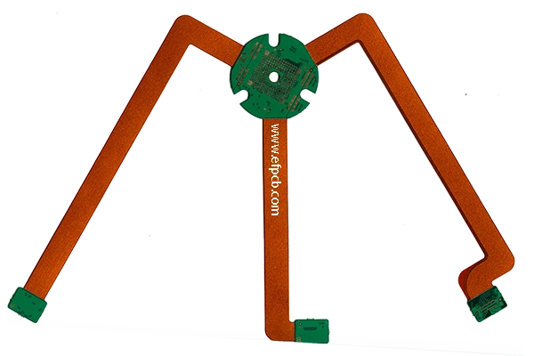
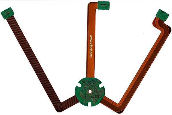
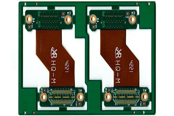
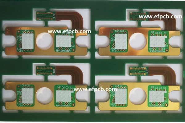
A rigid flexible PCB is a printed circuit board that combines both rigid and flexible layers into a design. The inflexible regions structurally support the components, and the flexible regions allow the board to flex or fold to offer a space saving and/or movable advantage. This combination makes rigid flexible PCBs a must-have for high-functionality compact electronics.
The choice of materials used in producing rigid flexible PCBs is equally critical in defining the reliability and performance of the final flexible application. Commonly used materials include:
The selection of the materials will depend on the needs of the particular application: thermal stability, flexibility, electrical specifications.
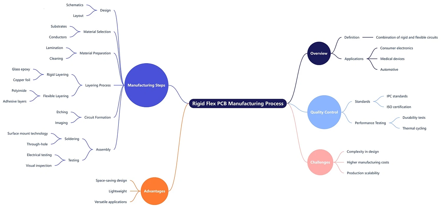
The production of a rigid flexible PCB is a multistep process, which demands accuracy and proficiency in each process. Here is a detailed summary of the process:
The circuit layout of the rigid flexible PCB is to be designed at first. The schematic and layout are created by engineers with sophisticated CAD tools, such as Altium Designer or KiCad. The design needs to include impedance control, bend radius, and layer stack-up to provide optimum performance.
It also involves prototyping to some extent. A prototype is made in order to test the effectiveness of the design - it can help in finding out any design flaws and in mass production. Material Preparation
Once you have the design completed, the materials for the hard and soft parts need to be made. Copper-clad laminates are used as the substrates, and polyimide films are added to the flexible region. Glues are used to affix the materials.
The prepared materials are also carefully screened for the absences of scratches or contamination that might adversely affect the final article.
Lamination is one of the most vital processes in the manufacture of rigid flexible PCBs. In that operation, the rigid and flexible ones are laminated to each other under heat and pressure to from layers. This tightens the layers into place, without stiffening the board up.
It is important to align during lamination so as not to have misregistration, which can cause poor connection or performance.
After lamination, the vias are drilled to connect various layers electrically. Laser drilling or mechanical drilling can be employed for this purpose, depending on the design.
After drilling of the holes, copper is plated into the holes in a process called through hole plating. This welding guarantees good electric contact between the sheets. Circuit Pattern Etching
The patterns of the circuits for the copper layers are formed by etching. A photoresist is sprayed on the board and circuit layout is transferred on the board by exposure to UV light (Optional). The exposed traces are chemically etched off leaving the desired copper traces.
Great accuracy is required in this stage in order not, to over-etch or under-etch otherwise circuit defects will occur.
A solder mask is deposited over the traces to prevent oxidation of the copper, and to insulate the traces from shorting while components are soldered in place, (FIG.6-5). The solder mask is traditionally green, although it can be a different color.
Screens are used to apply the solder mask onto the board and it is then cured with ultraviolet (UV) light or heat.
Surface finish keeps your board in the game (in terms of durability, solderability and long-term performance). Some common surface finishes for rigid flexible PCBs are:
Surface finish may be selected as required for the application.
The rigid flexible PCB is tested electrically before delivery to verify that it complies with standard design parameters. Continuity and impedance tests jobs are conducted to prove the board workability and reliability.
The last stage consists of a complete hand inspection of the board to fulfill the final quality inspection. Sporadic cutting-edge methodology including Automated Optical Inspection (AOI) and X-ray are used for identifying defects that are impossible to see with the unaided eyes.
Applications of Rigid flexible PCBs Rigid flexible PCBs are applied in many different areas and markets.
Their ability to incorporate hardness and softness makes them the perfect choice for space-saving designs with high reliability.
What are the advantages of rigid flexible PCBs?
Benefits of Rigid flexible PCBs Rigid flexible PCBs provide numerous benefits such as lighter and smaller designs, increased reliability, greater flexibility, and longer lasting life and performance in rugged and harsh environments.
What is the difference between a standard PCB and a rigid flexible PCB?
The combination of both rigid and flexible at the same board is called a rigid flexible PCB and the opposite end, standard PCBs are either all rigid or all flexible boards. This hybrid architecture enables the flexibility needed for advanced applications.
What are the difficulties in making of rigid flexible PCBs?
Among the challenging issues are the concerns of accurate alignment during the lamination process, consistent electrical connection, as well as durability of the flexible segments. Sophisticated methods of fabrication and control are necessary to deal with these problems.
How to control the quality of a rigid flexible PCB?
To maintain quality, consider working with a reliable manufacturer who uses the latest machinery and follows rigorous quality control standards. Rigorous testing and inspection is also essential.
Are rigid flexible PCBs cost-effective?
Even though a rigid Flex PCB has a higher one-time cost than that of a rigid PCB, its long-term reliability, space-saving characteristics, and durability usually translate into savings.
The production of rigid flexible PCBs is an intricate yet appealing mission. From design & material selection, through lamination and testing, each step of the process is critical to ensuring that the final product is of the highest quality and performance. With the best of both rigid and flexible PCBs, rigid flexible PCBs have revolutionized electronics and are a crucial solution when challenged with any combination of rigid and flexible circuit boards requiring innovative designs, in smaller packages.