-
Mail Us Todaysales@efpcb.com
-
Company LocationShenzhen, Guangdong, China
-
+86-755-23724206Call us for more details
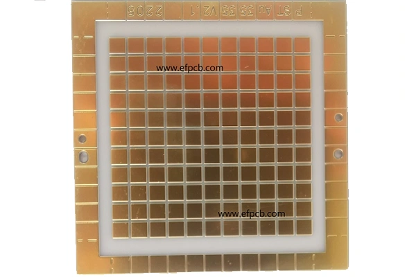
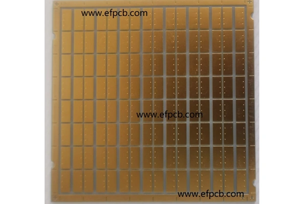
Part No.: E0297060159A
Layer count: 2 layer
Material: Ceramics Al2O3 + Copper
Minimum trace: >8 mil
Minimum space(gap): >8 mil
Minimum hole: 0.15 mm
Surface finished: immersion gold
Unit size 4.5*4.5mm
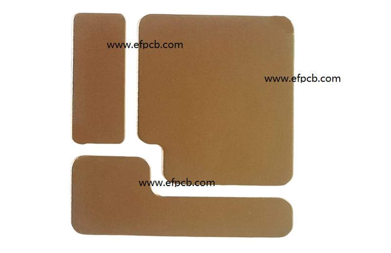
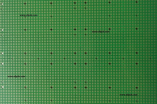
Ceramic substrate PCBs are a particular class of printed circuit boards where the base substrate is ceramic materials, unlike the typical FR-4 or metal substrates. Ceramic substrate PCBs have excellent thermal conductivity, strength, and isolation characteristics, so they are utilized for a long time in aerospace, automotive, telecommunications, and medical instruments. As a leading ceramic substrate PCB manufacturer, we provide high performances solutions suitable for these high end applications. This article will introduce you to how to produce ceramic substrate PCBs and how our products features.
Ceramic substrate PCBs refer to PCBs that are made of ceramic material as alumina (Al₂O₃), aluminum nitride (AlN), or silicon carbide (SiC) instead of the FR4 as the base layer. These offer excellent heat dissipation, high mechanical strength and good electrical properties and are natural choices for high power, high frequency or harsh environment applications.
Being a professional ceramic substrate PCB manufacturer, we are able to utilize these materials to create high quality PCBs for a wide range of challenging applications. We guarantee that our ceramic PCBs are of top quality with the best industry standards from material choosing to advance manufacturing.
Ceramic substrate PCBs have many advantages than ordinary PCBs, so they can be used in more special fields. Some features included are:
We are also a professional ceramic substrate PCB manufacturer, enabling you to take advantage of all of these attributes to produce robust, high function solutions for demanding applications.
The production of ceramic substrate PCBs demands particular methodologies and machinery for accuracy and excellence. What follows are the steps to develop these high-end PCBs.
Design and Simulation
The manufacture involves first designing the PCB layout and testing its performance. Ceramic substrate PCBs are challenging to design, they need tight thermal, signal and mechanical strength considerations. Our engineering team uses industry leading design software to produce layouts that are tailored to the specific characteristics of ceramic materials. This allows us to catch problems and make corrections on the PCB before we ever order prototypes. Material Selection and Preparation
It is all the more important to select the right ceramic material for the PCB. As the best ceramic substrate PCB manufacturer, we also provide different kind of ceramic materials such as alumina, aluminum nitride, silicon carbide etc. with the.
After the material is chosen, it is processed to required specifications for performance and reliability.
Laser Drilling and Via Formation
Drilling and via creation is important to link various PCB layers. We employ laser drilling technology in ceramic substrate PCBs to form accurate vias and holes. It is a sophisticated process that will help to achieve a high level of precision and protect the ceramic material from any harm. Laser Drilling is also critical for multilayer ceramic PCBs, as the precision needed to maintain signal integrity is essential.
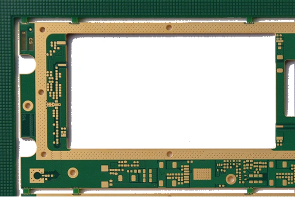
Circuit Pattern Printing
Unlike conventional PCBs, in circuit pattern printing on ceramic substrate PCBs are performed by using thick-film or thin-film technology. In thick-film processes, conductive pastes like silver, gold or copper are screen printed on the ceramic base and fired at high temperatures to build the circuit. Thin films are formed by depositing metal layers on the substrate via physical vapor deposition (PVD) or chemical vapor deposition (CVD). Both process are used for high accuracy and high durability circuit pattern.
Sintering and Lamination
Sintering is a vital stage in the production process where the ceramic body is subjected to elevated temperatures to bond the material and improve the mechanical and electrical characteristics. For multilayer ceramic PCBs, lamination is a process of applying heat and pressure to ensure bonding and proper registration of the layers. Advanced sintering and lamination processes assure the integrity and dependability of the finished product.
Surface Finishing
Surface finishing is also necessary to protect the PCB and allow for good soldering when assembling components. We can offer a range of types of finish including gold plating and nickel plating to suit the specific needs of various different application. These finishes improve the robustness and performance of the PCB while remaining compatible with the latest assembly technologies.
Quality Testing
Each ceramic substrate PCB that made by us is the subject of stringent quality testing to guarantee that it fulfils the top performance criteria. This involves thermal and electrical analysis, electrical testing, and evaluation of mechanical strength. As a quality-driven ceramic substrate PCB manufacturer, we guarantee every product that sent out from our factory is robust and good enough for working under harsh environment.
Why Should You Choose High Quality PCB as Your Ceramic substrate PCB Manufacturer?
Our firm distinguishes itself by our knowledge, technical know-how, and customer service. Here are just a few reasons why we are one of the top ceramic substrate PCB manufacturer in the industry:
Tailor-made Solutions: We know that every project is different. Our experienced engineers collaborate and support you in designing and manufacturing ceramic PCBs that best suit your needs.
State of the Art Production: We purchase the best machinery and processes money can buy to produce our products precisely and efficiently throughout the whole production.
Superior Quality: High quality is the essence of all our work. We process strict quality check from raw material to final testing, to ensure the stability and high quality of our PCB products.
Quick Turnaround: We know how important it is to meet timelines. With our efficient production workflow, we can ensure short lead time for ceramic substrate PCB without ever compromising on quality.
These profiles enable our engineer and technician to provide full support during your design and manufacturing process.
Ceramic substrate PCBs are widely utilized in applications that require high performance and have high reliability. Typical applications are as follows:
With our vast experience as a ceramic substrate PCB supplier, we have a proven track-record in delivering solutions to these sectors, enabling our customers to realize higher performance and reliability in their products.
IPC-2618B may be too when you consider what is involved in manufacturing ceramic substrate PCB. As a trusted ceramic substrate PCB manufacturer, we are driven by expertise, innovation and state-of-the-art technology to provide solutions for extreme challenges. Whether you are looking for custom designs, quick production, or expert advice, we can help. Contact us today to discover more about how we can meet your ceramic PCB requirements.