-
Mail Us Todaysales@efpcb.com
-
Company LocationShenzhen, Guangdong, China
-
+86-755-23724206Call us for more details

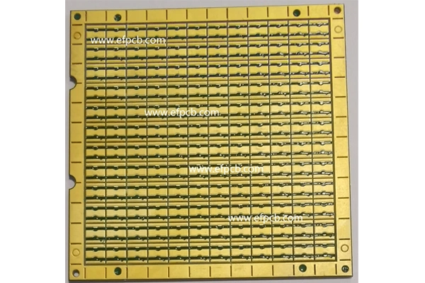
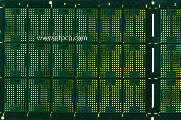
Part No.: E0277060129A
Layer count: 2 layer
Material: Ceramics + Copper
Minimum trace: 8 mil
Minimum space(gap): 5 mil
Minimum hole: 0.20 mm
Surface finished: immersion gold
Unit size 3.5*3.5mm
In the field of high-application potentials nowadays, a ceramics substrate PCB technology is widely used in heat dissipation, electrical insulation, and reliable application products. As a world class ceramics substrate PCB supplier, we focus on providing the highest quality custom ceramics PCB solutions to the most demanding automotive, aerospace, power electronics, and telecommunications industries. In this article, we will discuss the essential aspects of ceramics substrate PCB, including its features, advantages, the production process, and how come we are the best choice for your needs.
Ceramics substrate PCBs are PCBs that utilize ceramic material as the base substrate instead of the conventional fiberglass. These working temperatures are substantially higher than those tolerated by organic PCB substrates, such as for example FR-4.
This is good technology especially in applications where high power dissipation, thermal handling, and reliability are important. With our expertise in ceramics substrate PCB manufacturing, we offer customized solutions for industries that demand the utmost quality and performance.
High Thermal Conductivity
Heat dissipation is one of the outstanding characteristics of ceramic substrate PCBs. The thermal conductivity of ceramic materials such as aluminum nitride is much higher than that of traditional substrates, which has led to increased use in high-power applications such as LED lighting, power modules, and RF devices.
High Electrical Insulation
The electrical insulation of ceramics substrate PCBs is also not compromised when making it a critical attribute in keeping the security and dependability of electronics components. This enables the use of high power circuits without electrical break down or arcing.
Better Mechanical Stability
Rigid and strong ceramics are mechanical stress/vibration resistant and thus the quartz, porcelain and alumina based ceramics substrate PCBs are capable of sustaining harsh weather conditions. Therefore they are ideal candidates for tough environment applications including automotive, aerospace and industrial applications.
Compact and Lightweight Design
The exceptional thermal and electrical characteristics of ceramics substrate PCBs allow, electronics developers to create smaller and lighter products without compromising the performance of the product. This is essential in areas where size and weight are important.
Long-Term Reliability
Ceramic substrates resist heat, moisture and chemical attack making products that use them more durable and more reliable over time. Being the reliable ceramics substrate PCB manufacturer, we aim to deliver the most quality and durable product every time.
Fabrication of ceramics substrate PCBs need high precision machinery and expertise in the subject to maintain the quality. Our manufacturing process consist of:
Material Selection
The process starts with choosing the right ceramic material according to the application needs. They provide the best thermal, electrical, and mechanical properties.
Substrate Preparation
Using fresh advanced techniques, the ceramic substrate is processed to have a flat and consistent surface. This process is vital to securing a good adhesion of conductive layers and components.
Depositing the Conductive Layer
A layer of conductor, usually copper, is applied onto the ceramic substrate via screen printing, laser direct structuring, or sputtering. It is the layer where the traces that connect the electronic elements reside.
Circuit Patterning
The required circuit pattern is etched (or printed) on the conductive layer with high precision. This makes sure the PCB is functional and dependable.
Lamination and Finishing
Other layers like solder mask or protective coating – can be added for wear and performance resistance. The finished ceramic substrate PCB goes through strict quality control to make sure it is conforming to all the specifications.
We are known as top ceramics substrate PCB manufacturer providers for our innovative, uncompromising quality and unbeatable customer satisfaction. Here are a few reasons why we are the optimal choice for customers all over the world:
Ceramics substrate PCBs are used in various applications where the performance and reliability is critical. Typical applications include:
By collaborating with a trusted manufacturer of ceramics substrate PCBs, you can rest assured your products are utilizing the best technology available, delivering flawless performance in the most demanding environments.
The ceramic substrate PCB technology is changing the electronics industry with exceptional thermal conductivity, electrical insulation and mechanical reliability. These high-end PCBs are required for high performance applications where the conventional substrates are not sufficient.
As a top ceramics substrate PCB manufacturer, EFPCB is dedicated to providing innovative solutions for the changing requirements of our customers. Contact us today to discover more about what we can do for you and your products, and how we can help you take them to the next level.