-
Mail Us Todaysales@efpcb.com
-
Company LocationShenzhen, Guangdong, China
-
+86-755-23724206Call us for more details
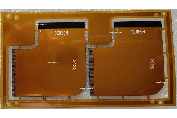
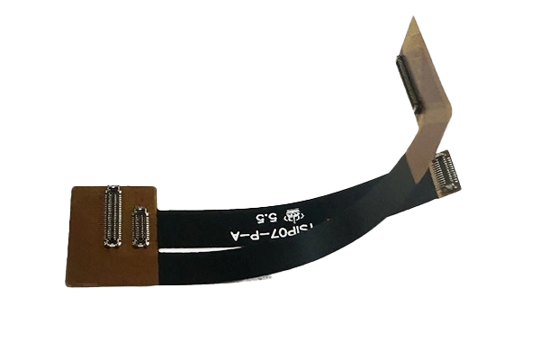
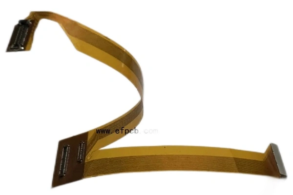
Part No.: E0275060171PCB
Layer count: 2 layer flexible PCB
Material: Polymide, 0.15mm, 0.5 OZ for all layer
Minimum trace: 5 mil
Minimum space: 5 mil
Minimum hole: 0.20mm
Surface finished: immersion gold
Panel size: 198*78mm/2up
Flexible circuits are designed for products that need to remain reliable as they are bent, folded or crammed into small spaces. What distinguishes a typical flex job from one that is production ready is process discipline at all levels, including material conditioning and the final electrical test. The following is a typical production flow for a flexible printed circuit board manufacturer, with highlighted portions which focuses on prevention of yield loss and long-term reliability.
The production of start with a concept of engineering. An expert Flexible Printed Circuit Board manufacturer analyzes the Gerbers, stack-up intent, impedance requirements, bend areas, and assembly limitations, then translates these details into a controlled traveler. Important planning check points are as follows:
Trace width and spacing capability vs. copper weight - Bend radius recommendations and copper balancing in dynamically active areas - Coverlay window dimensioning for pads, vias and test points - Panelizing methods to minimize stretch and maintain registration
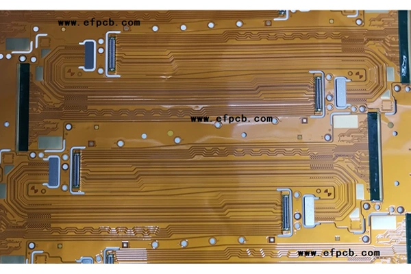
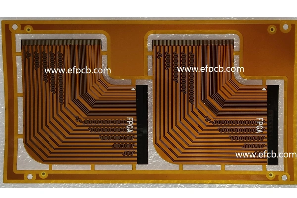
Raw material products, including polyimide copper clad laminates and bonding agents, are selected based on thermal and mechanical requirements. A trustworthy flexible printed circuit board manufacturer hold to the moisture, cleaness, surface activation prior to imaging begins. The circuit pattern is then established by photoresist coating, exposure and development, followed by copper etching to create traces. The tight etch control maintains line geometry and reduces the potential for opens or unintended impedance shifts. Drilling, Metallization, and Layer Bonding Drilling, Metallization, and Layer Bonding Component holes and vias can be drilled mechanically, by laser or a combination thereof, depending on the hole size. After drilling, desmear and conditioning treat the hole walls to make them ready for copper deposition. At this point a specialized FPC Manufacturer will care about even plating thickness as via reliability is a key parameter that often determines field life. Multilayer flex or rigid flex is constructed using lamination to bond the layers together at specified temperature and pressure cycles. Registration control in this case also directly impacts pad alignment, annular ring integrity and final assembly yields. Profiling coverlay is used to insulate and protect copper and to also insulate and maintain flexibility. Openings are precision cut to expose solder pads while eliminating the formation of stress risers around bend zones. When stiffeners are needed for connectors or component areas a Flexible Printed Circuit Board manufacturer attaches them using proven adhesives to enhance handling and assembly strength. The surface finish is chosen for solderability and shelf life, typically ENIG, immersion silver or OSP. The boards are then routed, laser cut or punched to their final outline and the edge is quality controlled to prevent tearing while flexing.
Leading flexible printed circuit (FPC) producers carry out short-circuit and open-circuit tests on every single product with dimensional inspection and microscopic cross section analysis for high reliability requirement. Clean packaging and sturdy backing, combined with anti-static shielding, preserve the outsides of the circuit boards from getting bent or wrinkled while in transit. Although it is not necessary for a manufacturer to be doing excellent processes to be able to provide good results, it is important that they be adequately process controlled at every stage I need to trust that the results I get from prototyping are going to be the same as I get from production.