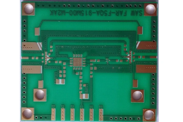
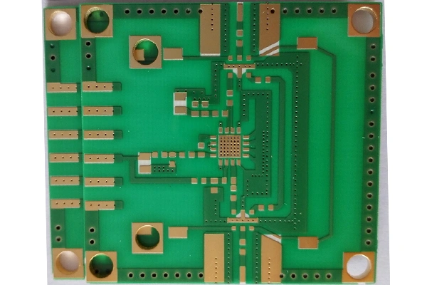
How to Manufacture High Frequency PCB?
High frequency PCBs are a vital part for those needs-based industries like telecom, aerospace, automotive, healthcare where signal integrity, low loss and high speed transmission are required. As a high frequency PCB manufacturer, we have more than 14 years experiences of high frequency PCB production and are able to tailor unique solutions to the requirements of these business sectors. In this post, you’ll find about how to high frequency PCB fabricating and designing with keeping in mind our hight tech Producing Procedure and the product functionality makes the difference in the Market.
What are High Frequency PCBs?
High-frequency PCBs are operated at frequencies usually higher than 1GHz. These PCBs are used for applications that need high speed signal transmissions, low signal distortions or low electromagnetic interference. Unlike typical PCBs, high-frequency PCBs require special material and specific manufacturing processes to perform under the required standards.
We have deep knowledge of designing and manufacturing of high frequency PCB, therefore we know how to achieve the highest productivity. Every process from raw material to the product is elaborately planned and controlled so as to conform to strict industry standards.
Materials Important High Frequency PCBs
A high frequency PCB foundation is its components. The dielectric constant (Dk), loss tangent (Df), and substrate’s thermal stability are important parameters to estimate the PCB performance in high frequency. Typical products are:
PTFE (Polytetrafluoroethylene): Because of its small Dk and Df, PTFE is suited for applications at high frequency.
Ceramic-filled substrates: They provide good thermal stability and mechanical strength.
Rogers laminates: Known for their stable electrical properties, they are decorative solutions for RF and microwave circuits.
As a premier high frequency PCB manufacturer and supplier, we utilize only the best materials in the production of your high frequency PCBs to guarantee superior results with high frequency PCB that are efficient and reliable in all respects. We have material expertise that enables us to provide with the tailored solution to meet particular application requirements.
Advanced Manufacturing Techniques
Manufacturing high frequency PCBs is a precision job and you cannot trust it to amateurs. It includes a number of important stages, and you should be precise and careful every step of the way. Here’s how we do it:
1. Design and Simulation
The first step in manufacturing the high frequency PCB is to design the layout and simulate the circuit performance. Using state of the art software our team designs circuits with excellent signal integrity and minimal loss. By analyzing the PCB's responses under different circumstances, we can find and correct the potential problems before the production.
2. Material Preparation
Once the design is frozen, then is the time to work out the substrate. As a manufacturer of high frequency PCBs, we are committed to using superior materials with low dielectric and low signal loss. Good preparation of materials underpins the high-frequency PCBs finishing.
3. Precision Etching
Etching is an important stage in defining the circuit patterns on the PCB. For high frequency PCBs, the accuracy must be ensured to prevent the signal distortion.. We can also use an advanced etching process to produce clean, precise traces for best results.
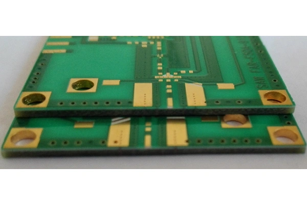
4. Layer Lamination
In order to keep the signal integrity across layers, the lamination of multilayer high frequency PCBs need stable pressing condition. Our lamination process is rigorously monitored to guarantee registration and to prevent interlayer contamination. This bit is important in which may apply to more complicated circuitry and high speed signals.
5. Drilling and Via Formation
Drill and via formation are critical for multistage circuit board connection. We are equipped with advanced technologies to produce microvias, through-holes with high accuracy. This allows for easier connection and less signal loss.
6. Surface Finishing
Surface finishing is also essential to the protection and performance of the PCB. We provide a variety of finishes such as ENIG (Electroless Nickel Immersion Gold) and HASL (Hot Air Solder Leveling) for different requirements and application.
7. Quality Testing
Each high frequency PCB we produce is tested thoroughly to meet the industry standard. We perform everything from impedance testing to thermal analysis to ensure we know our products inside and out.
What Sets Us Apart?
We are known in the industry as a reputable manufacturer of high frequency PCBs, eager to share our expertise and solutions. Here are some features of our products that set us apart from others:
Custom Solutions: We know that every application is different. Our team collaborates with customers to create custom PCBs to meet needs.
High-Tech: We use advanced technology and modern equipment, to provide you with quick and efficient service.
High Quality: We make quality the heart of everything we do. Our rigorous quality control allows us to say each and every PCB that we manufacture possesses a high level of performance and reliability.
Fast Turnaround: Today watch industries are more time sensitive than ever. We provide fast production cycles with no quality trade-offs, that’s why we are your best choice if you want high frequency PCB manufacturer. Expert Support Our engineering and technical team are the best in the industry and they make the design to production journey seamless for our customers.
Applications of High Frequency PCBs
High Frequency PCBs are essential and they have endless uses, and most industries rely on them. Some of these are:
Telecommunications In antennas, satellite systems, and wireless networks. Automotive: The need for radar systems in ADAS and autonomous vehicles.
Aerospace: Vital to navigation and communications.
Healthcare: used in medical imaging and diagnostic machines.
As a high frequency PCB manufacturer, we continually work with the strongest businesses in these industries to provide innovative, high-performance and dependable solutions that power advancement and growth.
Conclusion
In order to make high frequency PCBs, one must understand the materials, the technology and have an uncompromising attitude to quality. As a reliable and professional high frequency PCB manufacturer, we integrate knowledge, creativity and advanced machinery to satisfy even the most complex requirement. Should you have your own requirements or need our comprehensive products for your high-frequency projects, our dedicated team will be happy to support you. Contact us to discover more about how we can bolster your company.
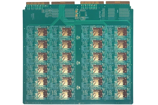
Telecommunication equipment application