-
Mail Us Todaysales@efpcb.com
-
Company LocationShenzhen, Guangdong, China
-
+86-755-23724206Call us for more details


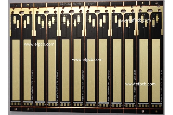
Part No.: M0115360179C
Layer count: 1 layer Metal Core PCB
Material: Copper core, 1.0mm, 1 OZ, 5.0 W/M*K
Minimum tack: 20 mil
Minimum space(gap): 25 mil
Minimum hole: 3.0mm
Surface finished: ENIG
Panel size: 258*188mm/12up
Characteristics: MCPCB, copper core PCB
Copper core PCB is widely used in high-performance electronic applications as it offers excellent thermal conductivity and reliability. Copper core PCB is a special kind of circuit board which use copper for the core instead of traditional FR4 or aluminum core, it can greatly improve the heat dissipation, and facilitate the miniaturization of electronic products. According to a 2023 IPC report, the thermal conductivity of copper core PCB can be as high as 400 W/mK, which is a higher level than the thermal conductance of standard FR4 boards with value 0.25 W/mK. This unique characteristic enables copper core system PCB to be the best choice for LED lighting, power electronics, automotive and aerospace applications.
Material Preparation
The production of copper core PCB begins with the purchase of the copper sheets of high purity, with thickness typically varies between 1.0mm to 3.0mm. The copper is the heat spreader and mechanical core of the PCB. The copper base's surface is treated to be free from oxides and dirt, and for good adhesion to the following layers during lamination.
Lamination and Dielectric Layer Application
A critical process in copper core PCB production is deposition of the dielectric layer. This insulating material, a high performance polymer or ceramic in most cases, is laminated to the copper core by advanced vacuum lamination processes. This ensures consistent thickness, low void content and high bond strength. The dielectric integrity is so important that industry standards such as IPC-6012D dictate it that way, because it plays a part in the electrical performance and reliability of the copper core PCB.
Circuit Image Transfer
After the dielectric layer is deposited, a sheet of copper foil is laminated over it. The circuit pattern to be formed on the copper foil is placed by photolithography. A photosenitive resist is coated, exposed through a mask to UV light and developed to stripes of resist revealing the circuit traces. This is an essential phase for the formation of the electrical paths of the copper core pcb.
Etching and Cleaning
The exposed copper foil is then etched with chemicals, such as ferric chloride or ammonium persulfate, to chemically remove the unprotected copper and leave the designed circuit pattern. The board is cleaned thoroughly after the etching process to remove the retardant agent and the reaction materials. This makes sure the copper core pcb can have good electric integrity and surface quality.
Drilling and Metallization
Vias and holes for component mounting and parallel treatment can be drilled by precision drills. For a copper core PCB, the via metallization is treated separately since the copper core can serve as a grounding plane or heat sink. Sophisticated processes such as plasma cleaning and electroless copper deposition are used to provide reliable electrical contacts and thermal paths.
Solder Mask and Silkscreen Application
Application of the solder mask In order to protect the circuit traces and prevent solder bridges when assembling a solder mask is applied. The silkscreen layer provides component labels and markings to facilitate assembly and maintenance. High temperature solder mask are usually applied in copper core PCB for high temperature application.
Surface Finish
To improve solderability and prevent oxidation, a number of surface finishes are used including ENIG (Electroless Nickel Immersion Gold), OSP (organic solderability preservative), HASL (Hot Air Solder Leveling). The selection of finish is based on the application and performance requirement of copper core PCB.
Final Inspection and Testing
A series of tests and inspections are stringent to verify the copper core PCB is well within the specification. AOI, X-ray testing, and thermal cycling tests verify circuit, layer adhesion, and thermal performance. Thermal shock and electrical tests according to the UL standards must establish that copper core PCB is more reliable, proving that it is the best choice for harsh environment application.
Copper core PCB provides superior thermal, electrical and mechanical performance. The heat spreading capability results in greater power densities, longer component lifetimes, and lower probability of thermal failure. Top producers of power electronics say device reliability improves 15-30% when using copper core PCB.
Copper core PCB products are often used in LED lighting modules, automotive power control units, RF amplifiers, aerospace avionics, etc. This technology will play a key role in next generation electronics thermal management for both performance and safety.
Fabricating copper core PCB is a complex processing of material science, aerospace engineering, and quality control. Its exceptional characteristics enable copper core PCB to meet the increasingly demanding requirements of modern day electronics subjected to thermal and reliability issues. With the increasing demand for high performance devices, the importance of copper core PCB will continue to grow and shape the innovation in the future of electronic designing and manufacturing.