-
Mail Us Todaysales@efpcb.com
-
Company LocationShenzhen, Guangdong, China
-
+86-755-23724206Call us for more details
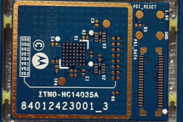
Part No.: E0615060179A
Layer count:6 layer HDI
Material: FR4, 1.0mm,0.5 OZ for all layer
Minimum track:3.8 mil
Minimum space: 3.5 mil
Minimum hole: 0.15mm
Surface finished: immersion gold + selective hard gold (Au>3UM)
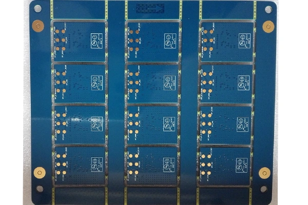
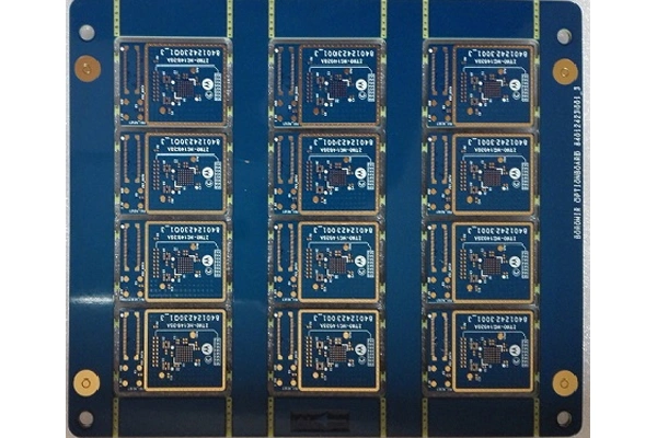
Panel size: 198*178mm/12up
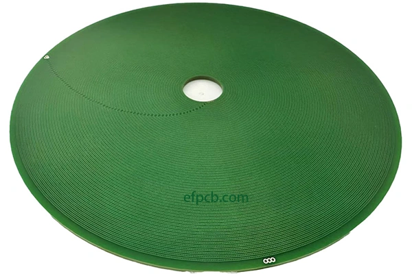
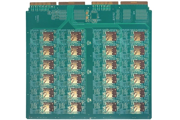
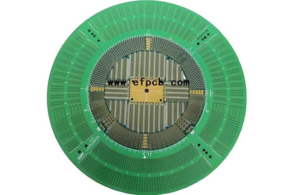
High-Density Interconnect (HDI) PCBs are after part in today’s advanced electronics. With compact size, high performance, and complex circuit support, they have been popular products in telecommunication, automotive, medical, and consumer electronics fields. As a reliable HDI PCB manufacturer, we provide you with innovative solutions that satisfy the requirements of modern technology.
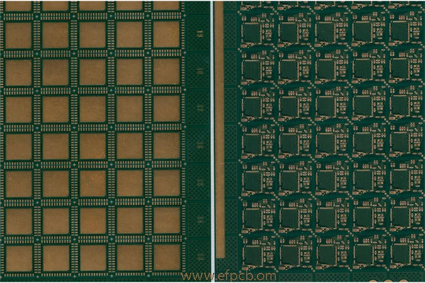
Is being HDI PCB manufacture good quality? High Density Interconnect PCBs (HDI) is a kind of a complex process. The process starts by choosing premium quality materials like thin dielectric layers or copper foils to make sure the board is capable of carrying the high-density circuits. Laser drilling is an essential stage in production. Microvias, small holes that connect two PCB layers, are drilled by lasers drilling technology. These microvias promote higher circuit density, which results to the compact design HDI PCBs are having. Being a professional HDI PCB Manufacturer, we utilize state of the art laser drilling machines for precision and dependability. Then, the layers are laminated together using the high pressure and high temperature. This ensures, among other things, good adhesion between the layers, which is essential for strength and so on for the finished PCB. Conventional electroplating is then used to build conductive paths inside the microvias for reliable electrical connections between layers. State-of-the-art imaging and etching processes are employed to produce the fine circuit patterns needed. To conclude with surface finishes can be deposited to protect the board and enhance solderability.
There are so many benefits of HDI PCBs over ordinary PCB. Because of their small size, devices can be made more compact and lighter, which is perfect for use in where-space applications. The high-density structure is conducive to faster signal transmission and reduction of signal loss that is critical for high speed and high-frequency devices. As a top HDI PCB manufacturer, we understand the value of dependability. Our products are engineered to perform reliably in harsh conditions and high stress environments, the ideal solution for innovative applications.
Why Choose High Quality PCB as Your HDI PCB Manufacturer?
Our company always upholds the work attitude to deliver HDI PCB of the highest quality according to your individual demands. With high-end manufacturing equipment and professional engineering team, we can provide the best solutions that meet the latest trend of the industry. We value precision and quality, and every HDI PCB is guaranteed to meet a strict set of performance and durability criteria. Whether your needs are for single-layer, multilayer, or stacked microvia configurations, our expertise as an HDI PCB fabricator will ensure superior results.
HDI PCBs are the foundation of current electronics, allowing for smaller, faster, and more energy-efficient appliances. It is important to choose the best HDI PCB manufacturer, so as to obtain the best performance and high reliability. Our expertise and experience make us the ideal choice you’re your manufacturing requirements. We are your trusted source for your high density interconnect PCB manufacturing requirements with over 18 years of experience and state of the art production facilities. Your HDI PCB is ready to get your finished product. With our innovative technology, rich experience and quality focus, we are the reliable one-stop service provider for all your needs. It is the right choice for your high performance needs of your life.