-
Mail Us Todaysales@efpcb.com
-
Company LocationShenzhen, Guangdong, China
-
+86-755-23724206Call us for more details
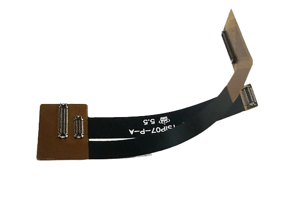
Part No.: E0215060176A
Layer count: 2 layer flex PCB
Material: Polymide, 0.13mm, 1/3 OZ for all layer
Minimum trace: 2.5 mil
Minimum space (gap): 2.5 mil
Minimum hole: 0.15mm
Surface finished: immersion gold
Panel size: 75*15.5mm/1up
Characteristics: Flexible PCB connector, 1mil Polymide, immersion gold, flexible PCB, flex connector
Flexible PCBs, the go-to solution for applications that require a thinner, lighter and more adaptable products, have been transforming the landscape of modern electronics. Whether it be medical wearables, automotive sensors or consumer electronics, this type of PCB is perfect for applications where traditional rigid boards would not fit or perform as well. But, just like for everything else, a quality is always counterbalanced by a corresponding drawbacks, and the unique properties of flexible PCBs require special care and design choices to ensure manufacturability, reliability and cost-efficiency. In our article for today, we will be going over these 10 best practices that can optimize your flexible PCB design for your application.
1. The choice of an Optimal Substrate
The choice of the correct base material is the base of a reliable flexible PCB. Polyimide has been the substrate of choice for most flexible PCB designs, offering the dual qualities of thermal stability and flexibility. For projects under a tighter budget and for which thermal resistance is less of a critical issue, PET is also a valid choice.
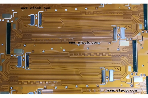
2. Trace Routing
Trace Routing is a vital aspect of all PCB designs. But for flexible PCBs, poor routing can cause stress concentration, signal loss and mechanical failure:
3. Minimum Bend Radius
Make sure your flexible PCB will not be bending beyond the minimum bend radius. Exceeding this radius can damage both the copper and the substrate.
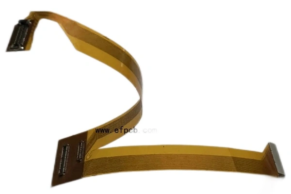
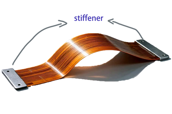
4. Stiffeners
You will want to reinforce the connector zones and component pads of your flexible PCB to accommodate the bending:
5. Component Placement and Pad Design
For the assembly process of your flexible PCB, position your components to avoid flex-induced stress.
6. Via Design and Placement for Flexible PCBs
The design, placement, and types of vias will end up affecting manufacturability of your flexible PCB:
7. Optimizing Panelization and Tooling
Smart panelization and tooling strategies can make your production process much more efficient:
8. Coverlays and Solder Mask Parameters
Coverlays protect the circuitry on a flexible PCB. It is usually a polyimide film with adhesive.
9. Communication with your Manufacturer
Engage with your manufacturer early on in the design process of your flexible PCB. This will not only save time but also reduce errors. Manufacturers should know the optimal stack-ups, materials and layout rules from experience, and can give you good advice for making a more manufacturable board.
10. Prototyping and Testing for Flexible PCB
Always prototype and test your prototypes. Simulate real-world flexing, thermal cycling and assembly processes so as to catch potential issues before pushing on to production.
Manufacturability is much more crucial to the design of flexible boards than our conventional rigid boards. In order to endure repeated bending or twisting, a flexible PCB relies on thin, bendable materials like polyimide or polyester film. These materials open new design possibilities but also present unique challenges for the manufacturing process. A designer must keep these problems in mind when designing a flexible PCB, and do their best to optimize for an efficient and defect-free fabrication.
In our article for today we went over 10 tips for designing your flexible PCB in the mindset of DFM, tips that will help your product remain robust in high-volume production, meet reliability standards and avoid unnecessary cost drivers. Following these best practices and collaborating closely with your manufacturer, you’ll ensure that your flexible PCB project is the success that it should be: delivering innovative products that perform as intended and are manufacturable at scale.
Medical devices